




Engineering three-dimensional network of SiC nanowire aerogels for efficient electromagnetic wave absorption: a review
 0
0 Abstract
Achieving high-performance electromagnetic wave (EMW) absorption remains fundamentally constrained by the intrinsic trade-off between impedance matching and efficient attenuation. This review presents SiC-based ceramic nanowire aerogels as a transformative platform to decouple this trade-off. These flexible ceramic aerogels leverage ultrahigh porosity (> 90%) to lower effective permittivity for improved impedance matching, while their interconnected nanowire architectures provide abundant interfaces and conductive pathways for multi-scale polarization and resistive dissipation. By synergistically combining lightweight design, high-temperature stability, and frequency agility, silicon-based ceramic nanowire aerogels offer a versatile platform for next-generation EMW absorption. We discuss recent advances in 3D network engineering of SiC nanowire aerogels, including compositional optimization to enhance attenuation, impedance gradient design to achieve broadband absorption, and dynamic frequency tuning enabled by compressible elasticity. Finally, we outline future directions, including programmable multi-scale architectures, closed-loop adaptive absorbers, multifunctional integration, scalable manufacturing, and high-temperature magnetic-dielectric multiphase systems.
Keywords
INTRODUCTION
The rapid proliferation of electromagnetic (EM) technologies in military stealth, EM compatibility, 5G/6G wireless communications, and civilian EM protection has driven an increasingly urgent demand for advanced electromagnetic wave (EMW) absorbing materials with superior performance[1-6]. Efficient EMW absorption requires the simultaneous fulfillment of two inherently conflicting criteria: impedance matching at the absorber–air interface to maximize wave penetration into the material interior, and strong attenuation capability to efficiently dissipate the absorbed EM energy into heat[1,4,5,7]. However, impedance matching requires the material’s permittivity and permeability to closely approximate unity, whereas strong attenuation relies on high dielectric or magnetic loss, imposing opposing requirements on the material’s intrinsic EM properties[4,5,7]. Reconciling this fundamental impedance–attenuation conflict within a single material or structural system to achieve broadband, strong-absorption, lightweight, and environmentally robust EMW absorption remains the central scientific challenge in the field[5,7].
Extensive efforts have been devoted to resolving this impedance–attenuation conflict through diverse absorber material families. Magnetic loss materials such as ferrite and carbonyl iron, benefiting from recent advances in morphology engineering and heterostructure design, have achieved significantly enhanced absorption bandwidth and intensity[8]; however, their high densities (> 3 g/cm3), Snoek’s limit-constrained permeability, skin effect, and magnetic degradation above the Curie temperature limit their use in lightweight and high-temperature applications[7-10]. Carbon-based absorbers including graphene, carbon nanotubes (CNTs), and MXene offer high dielectric loss and excellent designability, with hybrid MXene/graphene aerogels incorporating magnetic components achieving minimum reflection losses beyond -70 dB[11-15], yet excessive conductivity causes impedance mismatch and oxidative degradation above 600 °C restricts high-temperature use[16]. Polymer-derived composites provide flexibility and strain-tunable absorption[17,18], but matrix decomposition below ~500 °C precludes extreme-environment deployment. SiC-based ceramics exhibit tunable dielectric properties from stacking-fault dipole polarization and wide bandgap[19-23], yet in dense or powder form EM parameter tailoring remains difficult and brittleness limits structural adaptability[24-26]. These limitations collectively underscore that compositional optimization alone cannot simultaneously satisfy broadband impedance matching, strong attenuation, and high-temperature stability[27,28].
Constructing low-dimensional building units into macroscale 3D porous aerogel networks has emerged as a transformative structural strategy to decouple the impedance–attenuation conflict[29,30]. Ultrahigh porosity
Among all-ceramic candidates, SiC nanowires are uniquely advantageous as building units for aerogel absorbers. The abundant stacking-fault defects inherent to 3C-SiC nanowires act as dipole polarization centers that strongly enhance dielectric relaxation loss[20,23,46], while the large aspect ratio and one-dimensional morphology facilitate long-range conductive network formation, extending carrier transport paths and promoting interfacial polarization[6,23]. Nevertheless, the relatively high permittivity of SiC can lead to impedance mismatch when used alone. Incorporating low-dielectric wave-transparent phases such as Si3N4 or SiO2 into SiC aerogel frameworks offers an effective route to reconcile this mismatch, broadening the impedance-matched frequency window while preserving strong attenuation[47,48]. Beyond solid wave-transparent phases, void-based architectures such as engineered air interlayers between carbon fibers and SiC nanofibers (NFs) have recently been demonstrated to provide ultralow-dielectric impedance buffer regions, further extending the conceptual scope of the wave-transparent strategy[49]. Unlike rigid conventional ceramic absorbers, flexible SiC-based nanowire aerogels exhibit compressible elasticity, enabling dynamic tuning of absorption frequency bands via mechanical modulation of density and thickness. Although this capability was first demonstrated in carbon-based foams, it is particularly advantageous for ceramic systems operating under extreme thermomechanical conditions.
As shown in Figure 1, this review focuses on three-dimensional SiC nanowire aerogels (SNWA) and their composite systems incorporating Si3N4 wave-transparent components, and provides a comprehensive overview of recent advances in the design and optimization of their EMW absorption performance through 3D network engineering[22,50-53]. Specifically, we discuss: (1) compositional optimization strategies for enhancing EM attenuation in SiC nanowire aerogel networks, including conductive carbon coating, magnetic component incorporation, and wave-transparent Si3N4 and SiO2 phase introduction; (2) impedance gradient design through alternating multilayered aerogel architectures for broadband high-temperature absorption; and (3) dynamic absorption frequency tuning enabled by the compressible elasticity of flexible ceramic nanowire aerogels, establishing quantitative strain–frequency relationships for intelligent adaptive EMW absorption.
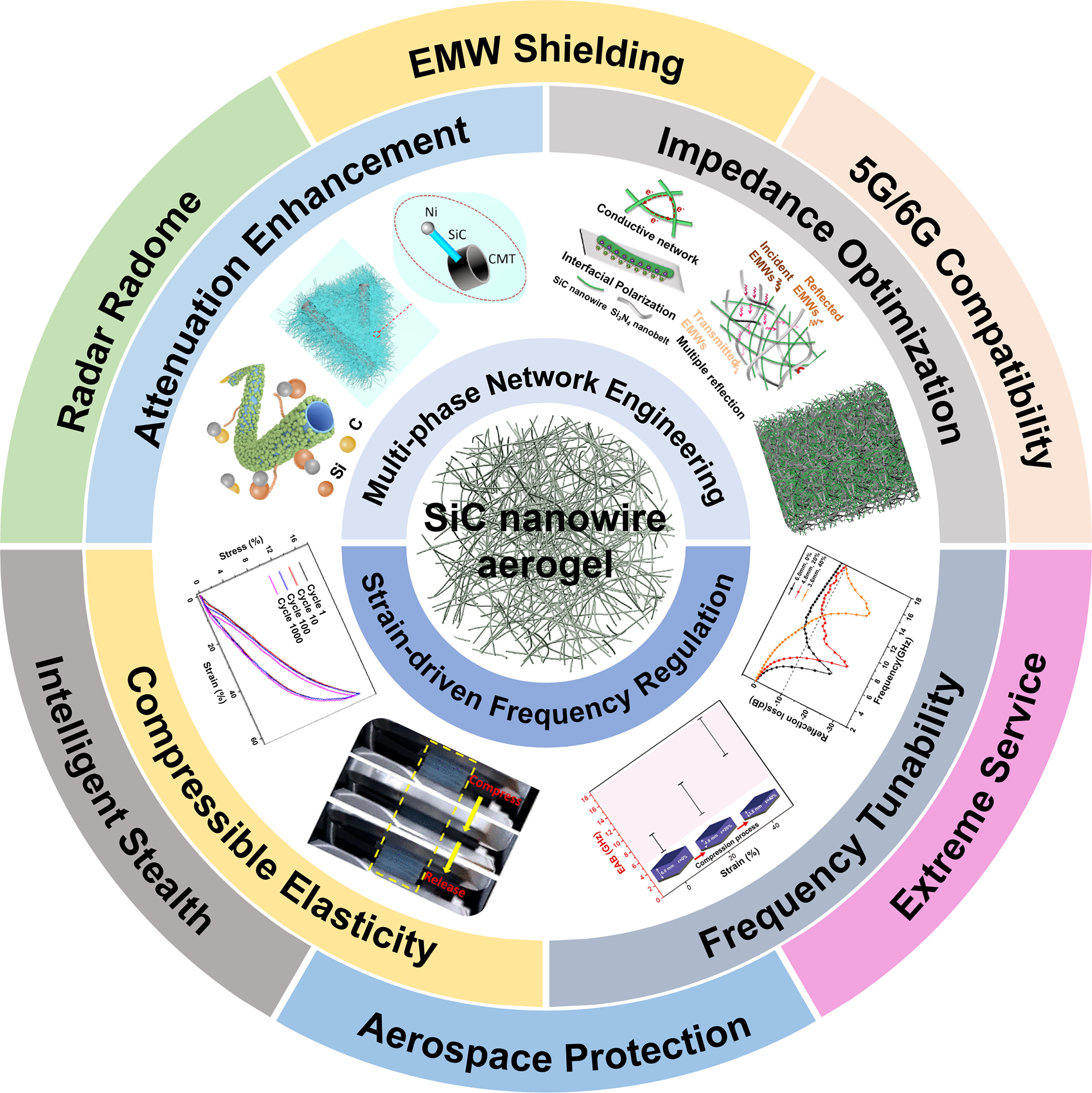
Figure 1. Schematic illustration of this review. Reprinted with permission[22,50-53]. Copyright © 2018 American Chemical Society; Copyright © 2022 Elsevier; Copyright © 2025 American Chemical Society; Copyright © 2022 Wiley-VCH; Copyright © 2025 The Author(s). CMT: Carbon microtube; EMWs: electromagnetic waves; EAB: effective absorption bandwidth.
COMPOSITIONAL OPTIMIZATION FOR ENHANCING EM ATTENUATION
To clarify how three-dimensional porous architectures reconcile the impedance–attenuation conflict, the standard absorber framework is briefly recalled[54]. The reflection loss is governed by the normalized input impedance of a single-layer absorber backed by a perfect electric conductor:
with effective absorption requiring Zin close to unity. The energy dissipation inside the absorber is quantified by the attenuation constant:
In dense ceramic absorbers, raising ε′′ to enhance α inevitably raises ε′ as well, pushing Zin away from unity. In a 3D nanowire aerogel with porosity P, an effective-medium description in which the effective real permittivity scales approximately with the solid volume fraction, ε′eff ≈ 1 + (1 - P)(ε′solid - 1), drives ε′eff close to unity at high porosity (P > 90%) and brings Zin toward 1. In contrast, ε′′eff is dominated by conduction along the connected nanowire network, interfacial polarization at heterointerfaces, and dipole polarization from 3C-SiC stacking-fault defects, all of which are largely preserved as long as network connectivity is maintained. The two parts of εeff are thus partially decoupled, providing the physical basis for the strategies reviewed below.
Although 3C-SiC stacking-fault dipole polarization has been widely invoked as a key loss origin in SNWA, its relative contribution varies across fabrication routes. In pristine SNWA with negligible amorphous coating, Cole–Cole plots typically exhibit one or two well-resolved semicircles attributable to dipole polarization, indicating that stacking-fault relaxation is indeed dominant. In conductive-coated systems such as SiC@C[55] and C/SiC-polypyrrole (PPy)[56], an additional linear tail at low frequency signifies a strong conduction loss contribution superimposed on dipole relaxation, and the relative weight of stacking-fault polarization is correspondingly reduced. In hybrid networks involving heterointerfaces such as SiC/Si3N4[47,52], SiC/SiO2[57], and SiC/Ni@CMT[50], multiple overlapping semicircles point to interfacial polarization as a comparably important contributor. A consolidated mechanism comparison across all reviewed systems is summarized in Table 1.
Comparison of representative silicon-based ceramic nanowire aerogel systems for EMW absorption
| Material system | Strategy | Density (mg·cm-3) | Thickness (mm) | RLmin (dB) | EAB (GHz) | Tmax (°C) | Loss mechanism | Ref. |
| SiC@C nanowire aerogel | AE-C/DT | 36-108 | 3.2-9.6 | -46.4 | 10.1 (static); 2.9-18 (strain-tunable) | - | CL + DP + IP | [55] |
| C/SiC-PPy NF aerogel | AE-C | 51 | 2.4 | -60.31 | 4.88 (7.6-12.48) | 1,000 | CL + IP + DP | [56] |
| Hollow SiC/C NFs | AE-C | - | 1.4/2.4 | -63.5 | 7.0 | 600 | IP + CL + MR | [58] |
| SiC nanowire/SiCNO composite aerogel | AE-C | 190 | 2.0/3.0 | -26.5/-31.9 | 5.2 | - | IP + MR + CL | [59] |
| SiC microtube/nanowire aerogel | AE-C | 51.3 | 2.0 | -56.39 | 6.04 | - | IP + CL + MR | [53] |
| SiC/Ni@CMT aerogel | AE-M | 5 | 3.2 | -41.5 | 10.1 | - | ML + CL + IP | [50] |
| Graphene/SiC nanowire/BN honeycomb aerogel | AE-M | - | 2.5 | -37.8 | 9.2 | 600 | IP + CL + ML | [61] |
| Magnetic graphene-SiCN aerogel | AE-M | 72.7 | 2.4 | -60.63 | 7.89 | 800 | IP + DP + ML + CL | [62] |
| C/SiC/SiBCN composite ceramic aerogel | AE-C | 116 | 2.8 | -45.7 | 5.3 | - | CL + IP | [63] |
| Dual-network Si3N4/SiC aerogel | IO/DT | 8-10 | 6 | -52.3 | 9.4 (static); 5.36-18 (0%-40% strain) | 1,000 | IP + DP + CL | [52] |
| SiC@SiO2 core–shell nanowire aerogel (SNWA-30) | IO | 36 | 3.65 | -57.22 | 9.4 (8.6-18.0) | - | IP + DP + CL | [57] |
| Alternating Si3N4/SiC multilayered aerogel | GM | 8 | 2.4 | -45.2 | 8.4 | 1,000 | Gradient impedance + DP + IP | [65] |
| Bifunctional SiC/Si3N4 composite aerogel | GM | 15 | 2 | -48.6 | 8.91 | 1,000 | CL + IP + DP | [47] |
| Gradient SiC/Si3N4 | GM | 15 | 3.6 | -46.2 | 11.2 | 1,300 | Gradient impedance + CL + DP + MR | [51] |
Silicon-based ceramic nanowire-assembled 3D networks have been employed as building blocks to develop a series of high-performance silicon-based ceramic aerogels through compositional optimization and structural design. Systematic investigations into the structural design and fabrication of these nanowire-based 3D networks, their regulation of EM parameters, and the dependence of dielectric-mechanical-high-temperature stability on macro-microstructural features have revealed the key factors governing EMW attenuation and loss. These studies encompass the effects of macro-microstructural and compositional gradients on EM parameters, dynamic quantitative relationships between material deformation, density-thickness, and absorption frequency bands, and ultimately lead to design strategies for optimizing EMW absorption performance.
Enhancing attenuation via conductive component incorporation
To strengthen the EMW dissipation capability, SiC nanowire-based 3D network aerogels were tailored in both composition and microstructure through the introduction of high-loss components. This approach achieves synergistic regulation of attenuation and impedance. As shown in Figure 2A-C, a conductive attenuation-type SiC@C aerogel was fabricated by coating carbon layers on SiC nanowire surfaces through glucose solution impregnation, drying, and carbonization processes[55]. With increasing carbon content (from 0 wt.% to 54 wt.%), the EMW absorbing capacity of the SiC@C aerogel initially improved and then declined. At a bulk density of 108 mg/cm3, the SiC@C aerogel attains an optimized effective absorption bandwidth (EAB) of 10.1 GHz, confirming its broadband and highly efficient EMW dissipation capability. This outstanding absorbing behavior is attributed to multi-scale (macro-, micro-, and nano-scale) loss pathways throughout the dielectric SiC@conductive C nanowire 3D network, where multiple attenuation mechanisms operate synergistically.
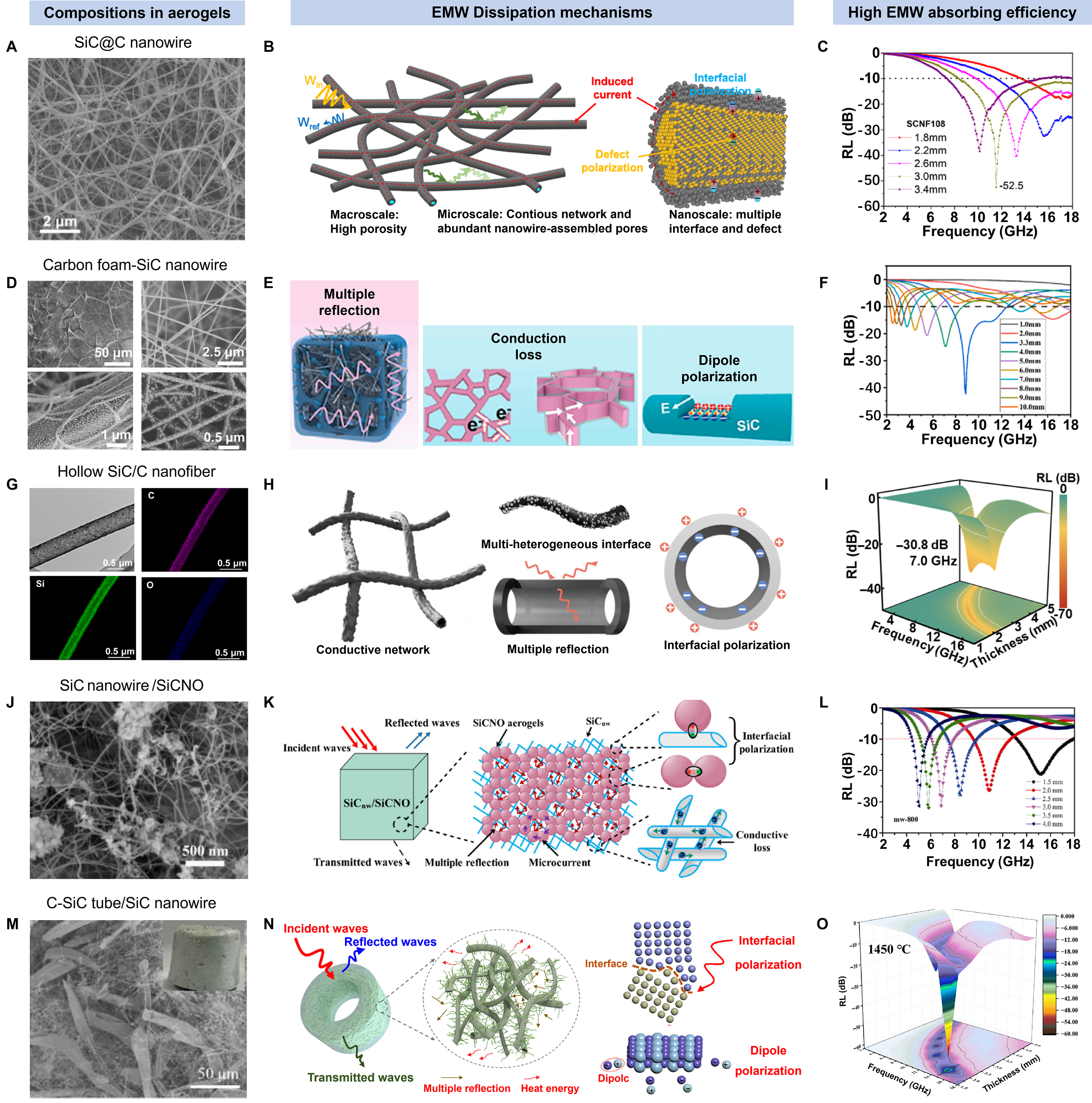
Figure 2. Conductive component incorporation strategies for enhancing EMW attenuation in SNWA. (A) SEM morphology, (B) multi-scale dissipation mechanism, and (C) reflection loss of SiC@C nanowire aerogel. (A-C) are reprinted with permission from Ref.[55]. Copyright © 2020, American Chemical Society; (D) SEM morphology, (E) absorption mechanism, and (F) reflection loss of C/SiC NF aerogel. (D-F) are reprinted with permission from Ref.[56]. © 2024 Elsevier; (G) EDS mapping, (H) conductive network and interfacial polarization mechanism, and (I) reflection loss of hollow SiC/C NF. (G-I) are reprinted with permission from Ref.[58]. © The Author(s) 2026; (J) TEM morphology, (K) absorption mechanism, and (L) reflection loss of SiC nanowire/SiCNO composite aerogel. (J-L) are reprinted with permission from Ref.[59]. © The Author(s) 2021; (M) SEM morphology, (N) absorption mechanism, and (O) high-temperature reflection loss of SiC microtube/nanowire aerogel. (M-O) are reprinted with permission from Ref.[53]. © The Author(s) 2025. EMW: Electromagnetic wave; SNWA: SiC nanowire aerogels; SEM: scanning electron microscopy; NF: nanofiber; EDS: energy-dispersive X-ray spectroscopy; TEM: transmission electron microscopy; RL: reflection loss; SCNF: SiC@C nanowire foam.
Beyond simple surface modification, template-derived strategies enable the construction of more complex conductive architectures. Song et al. fabricated a carbon-coated SiC NF aerogel via in situ chemical vapor deposition using carbon foam as both template and carbon source[56]. To further enhance EMW absorption, PPy was coated onto the C/SiC surface through impregnation and chemical polymerization, forming a conductor–semiconductor–conductor hierarchical structure. This design markedly enhances impedance matching and activates diverse dissipation channels, encompassing interfacial and dipole polarization as well as conduction loss. The resulting composite aerogel achieves an RLmin as low as -60.31 dB at a characteristic frequency of 2.96 GHz, indicating exceptional low-frequency absorbing performance [Figure 2D-F].
Structural engineering through hollow architecture design offers another route to simultaneously optimize impedance matching and enhance attenuation. Chen et al. synthesized hollow SiC/C nanofibers (H-SiC/C NFs) via a combined hydrothermal and carbothermal reduction approach[58]. The hollow architecture, combined with the residual carbon matrix and abundant SiC/C heterointerfaces, jointly facilitates impedance optimization and strengthens both interfacial polarization and conductive dissipation. The resulting H-SiC/C NFs deliver an RLmin reaching -63.5 dB at merely 1.4 mm thickness, with an EAB spanning 7.0 GHz at
Rather than introducing carbon externally, in situ growth of SiC nanowires within a dielectric matrix represents an internally built conductive network strategy. Yuan et al. developed a SiC nanowire-reinforced SiCNO composite aerogel via catalyst-assisted microwave heating at ultra-low temperatures[59]. The in situ formation of SiC nanowires throughout the polymer-derived SiCNO framework generates abundant heterogeneous interfaces while reinforcing the conductive pathway. The resulting composite aerogel delivers an RLmin of -26.5 dB centered at 10.9 GHz, accompanied by an EAB of 3.2 GHz at 2.0 mm thickness, where the absorption enhancement is principally ascribed to optimized impedance conditions, multiple internal reflections, and hopping-electron-induced microcurrents [Figure 2J-L].
At the highest level of structural complexity, bio-templated approaches can generate hierarchical multi-scale architectures. Zhang et al. designed a hierarchical porous SiC microtube/nanowire composite aerogel derived from natural kapok fibers via an in situ conversion strategy[53]. This unique microtube–nanowire heterostructure not only constructs a highly porous architecture but also facilitates multiple interfacial polarizations and conductive loss pathways. The resultant aerogel attains an
Beyond conventional conductive component incorporation, architecture engineering combined with composition design offers a further avenue to optimize the EMW absorbing performance. As shown in Figure 3, SiC@C nanowire metastructure aerogels were fabricated by depositing graphene-like carbon layers onto 3D-printed SiC nanowire scaffolds via chemical vapor deposition (CVD). The resulting aerogel exhibits an ultralow density of
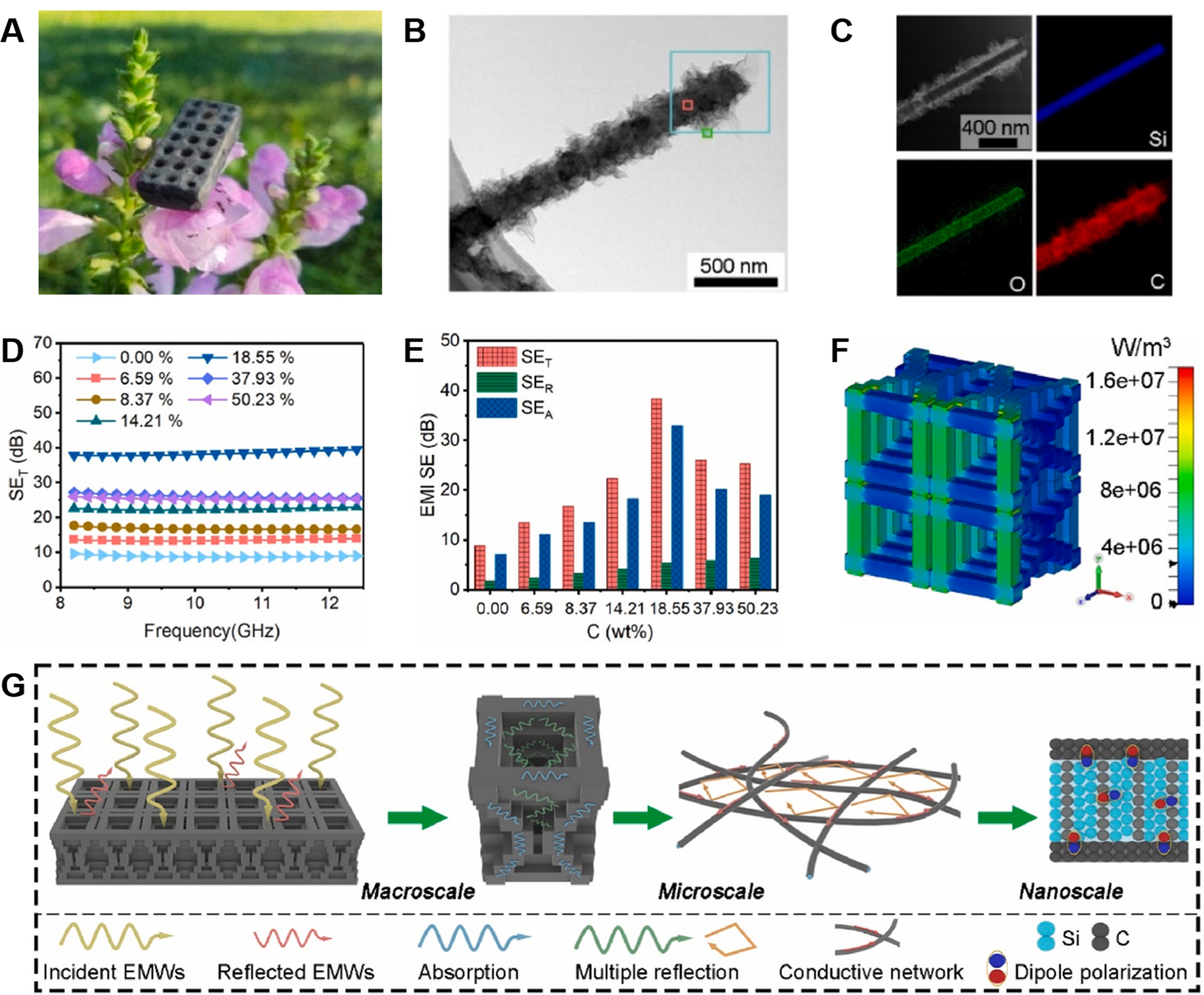
Figure 3. Robust SiC@C nanowire aerogel metastructures for EMI attenuation: (A) Optical image of the ultralight metastructure aerogel; (B) TEM image of an individual SiC@C nanowire; (C) HAADF-STEM micrograph with EDS elemental distribution maps; (D) Total EMI SE (SE_T) of metastructure aerogels at varying carbon contents; (E) SE_T, SE_R, and SE_A vs. carbon content; (F) Simulated power loss density distribution of the metastructure; (G) Multi-scale EMI attenuation mechanism from macroscale to nanoscale. (A-G) are reprinted with permission from Ref.[60]. © 2024 Elsevier. EMI: Electromagnetic interference; TEM: transmission electron microscopy; HAADF-STEM: high-angle annular dark-field scanning transmission electron microscopy; EDS: energy-dispersive X-ray spectroscopy; EMWs: electromagnetic waves.
Collectively, these studies demonstrate that conductive component incorporation strategies have evolved from simple surface coating to template-derived, hollow-structured, in situ grown, and bio-templated architectures, progressively enriching the heterogeneous interfaces and multi-scale loss pathways within SiC nanowire aerogel networks, thereby enabling increasingly effective broadband EMW attenuation.
Enhancing attenuation via magnetic component incorporation
Although conductive component incorporation significantly enhances dielectric loss, the lack of magnetic loss limits further improvement in impedance matching and low-frequency absorption. Building upon this foundation, the wave-absorption performance of the aerogel was further optimized by introducing magnetic materials into the dielectric-conductive composite aerogel system. As illustrated in Figure 4A, a three-dimensional network of low-density hollow carbon microtubes (CMTs) served as the framework. Using magnetic nickel (Ni) particles as catalysts, SiC nanowires were grown in situ via a chemical vapor deposition-like technique at 1,400 °C, resulting in a SiC/Ni@CMT aerogel with a 3D networked microstructure composed of SiC nanowires, Ni nanoparticles, and CMTs[50]. The results demonstrate that nickel nitrate serves a dual role as both a catalyst for nanowire growth and a regulator of the aerogel’s EMW absorbing behavior. When the nickel nitrate concentration was varied from 1 wt.% to 13 wt.%, the SiC nanowire population in the SiC/Ni@CMT aerogel first increased and then saturated, with a concurrent enlargement in nanowire diameter. Correspondingly, the absorption performance first improved and then deteriorated. At an optimal nickel nitrate concentration of 5 wt.%, the SiC/Ni@CMT aerogel attains an RLmin of -41.5 dB at
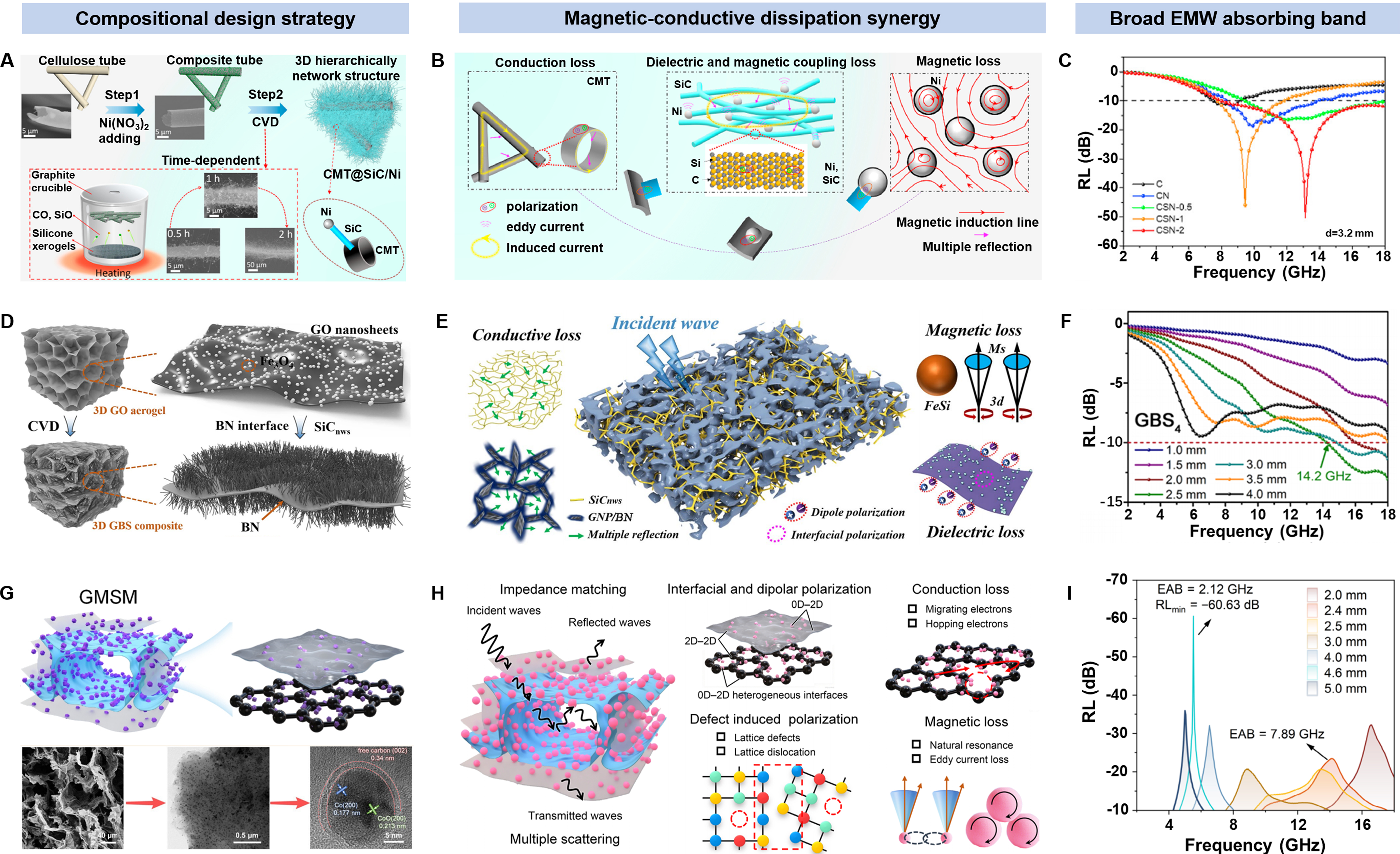
Figure 4. Magnetic component incorporation for enhanced EMW attenuation via magnetic-conductive-dielectric tri-network synergy. (A) Fabrication process; (B) multi-phase synergistic absorption mechanism, and (C) reflection loss of SiC/Ni@CMT aerogel. (A-C) are reprinted with permission from Ref.[50]. © 2022 Elsevier; (D) Microstructure, (E) absorption mechanism, and (F) reflection loss of graphene/SiC nanowire/BN honeycomb aerogel. (D-F) are reprinted with permission from Ref.[61]. Copyright © 2024, The Author(s); (G) Microstructure, (H) absorption mechanism, and (I) reflection loss of magnetic graphene–SiCN aerogel. (G-I) are reprinted with permission from Ref.[62]. © The Author(s) 2025. EMW: Electromagnetic wave; CMT: carbon microtube; BN: boron nitride; CVD: chemical vapor deposition; RL: reflection loss; GO: graphene oxide; GBS: composites: Graphene aerogel/BN/SiC nanowire composites; GNP: graphene nanoplate; GMSM: rGO@ZIF-67@polysilazane/ZIF-67; EAB: effective absorption bandwidth.
This magnetic-conductive-dielectric tri-network synergy concept has been further validated and extended in recent studies. You et al. constructed a hierarchical graphene aerogel with in situ grown SiC nanowires packed in a honeycomb structure, combined with BN interfacial layers[61]. The combined contributions of interfacial polarization, continuous conductive pathways, and magnetic-dielectric synergy yield an EAB reaching 9.2 GHz [Figure 4D-F]. Additionally, Yu et al. designed magnetically functionalized graphene–SiCN aerogels with hierarchical interfaces through a sequential confinement approach[62], attaining an RLmin of -60.63 dB and an EAB of 7.89 GHz through impedance matching optimization, multi-dimensional interfacial and defect-induced polarization, and combined magnetic-dielectric loss mechanisms [Figure 4G-I]. Furthermore, Jiang et al. prepared C/SiC/SiBCN composite ceramic aerogels by growing SiC NFs in situ within polymer-derived SiBCN matrices via chemical vapor deposition, reaching an RLmin of -45.7 dB, which further confirms that incorporating SiC nanowires into porous ceramic matrices effectively enhances multi-component EM dissipation[63].
Although compositional optimization through conductive and magnetic component incorporation has substantially enhanced the dielectric and magnetic loss capability of SNWA, the elevated permittivity arising from these high-loss phases inevitably compromises impedance matching at the absorber–air interface. Reconciling this conflict between attenuation enhancement and impedance matching requires a complementary structural-design strategy, in which low-dielectric wave-transparent phases and gradient impedance architectures are engineered into the 3D nanowire network, as discussed in the following section.
IMPEDANCE OPTIMIZATION AND GRADIENT STRUCTURAL DESIGN FOR BROADBAND ABSORPTION
Wave-transparent phase integration for impedance matching
The aforementioned studies demonstrate that incorporating EMW-transparent components into absorber systems can further optimize absorption efficiency and bandwidth through improved impedance matching. The fundamental basis for this strategy lies in the intrinsic ultralow dielectric properties of wave-transparent phases. Under optimized preparation conditions via a template-assisted precursor pyrolysis method, by controlling the mass ratio of siloxane sol to carbon felt, a low-dielectric Si3N4@SiO2 nanowire aerogel with minimal impurities and superior performance was successfully synthesized[64]. This aerogel exhibits exceptional high-temperature wave-transparent integrated properties, including an ultralow density
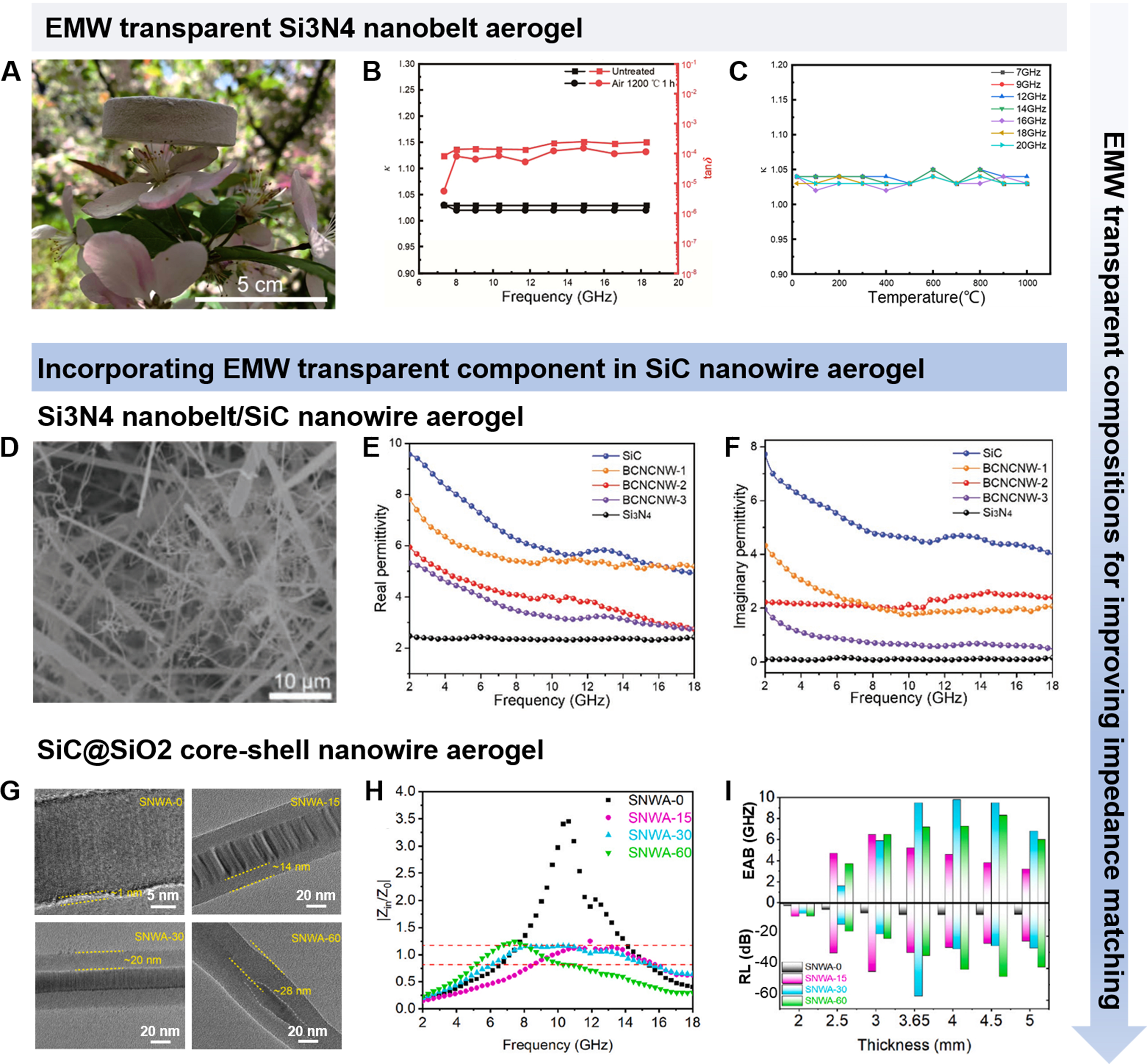
Figure 5. Wave-transparent phase integration strategies for optimizing impedance matching. (A) Macro/microstructure morphology, (B) dielectric properties, and (C) high-temperature dielectric stability of Si3N4@SiO2 nanowire aerogel. (A-C) are reprinted with permission from Ref.[64]. © The Author(s) 2023; (D) SEM morphology, (E) real permittivity, and (F) imaginary permittivity of dual-network Si3N4/SiC aerogel. (D-F) are reprinted with permission from Ref.[52]. © 2022 Wiley‐VCH GmbH; (G) TEM images of SiC@SiO2 core-shell nanowires with varying oxidation durations, (H) impedance matching characteristics, and (I) RL curves and EAB comparison of SiC@SiO2 nanowire aerogel. (G-I) are reprinted with permission from Ref.[57]. © 2023 Elsevier. SEM: Scanning electron microscopy; TEM: transmission electron microscopy; RL: reflection loss; EAB: effective absorption bandwidth; EMW: electromagnetic wave; SNWA: SiC nanowire aerogels.
Building upon this ultralow-dielectric foundation, an effective approach to optimize impedance matching in SiC aerogels is to introduce an independent wave-transparent second phase into the nanowire network. As shown in Figure 5D-F, wave-transparent Si3N4 phases were introduced into the SiC nanowire aerogel by regulating the reaction atmosphere during material preparation, yielding an impedance-optimized dual-network Si3N4/SiC aerogel with a reduced dielectric constant[52]. The results indicate that: (a) With increasing nitrogen pressure, the Si3N4 content in the composite aerogel gradually rises. Both the real and imaginary permittivity of the dual-network Si3N4/SiC aerogel diminish, while the absorbing performance first improves and then degrades. At a nitrogen pressure of 0.2 MPa, the dual-network aerogel containing 44 wt.% Si3N4 attains an EAB of 8.6 GHz with an RLmin of -52.3 dB; (b) The optimized dual-network Si3N4/SiC aerogel exhibits impedance coefficients exceeding 0.6 across the 10-15 GHz frequency range, reaching optimal impedance matching (close to 1) at 11.36 GHz; (c) At a bulk density of 10 mg/cm3, the aerogel reaches a peak EAB of 9.4 GHz.
Rather than introducing an additional second phase, in situ formation of a wave-transparent sheath directly on SiC nanowire surfaces represents an alternative route that achieves impedance optimization at the nanoscale interface. Wang et al. achieved this by controlled oxidation modulation of SNWA. Specifically, high-purity SNWA were first prepared through catalyst-free CVD under ambient pressure[57]. The amorphous SiO2 shell thickness was then systematically regulated by varying the oxidation duration at 900 °C (0-60 min), producing samples SNWA-0 (~1 nm sheath), SNWA-15 (~14 nm), SNWA-30 (~20 nm), and SNWA-60 (~28 nm, with complete oxidation of finer nanowires) [Figure 5G]. This oxidation modulation strategy enables a dual-function optimization: the wave-transparent SiO2 sheath markedly improves impedance conditions by facilitating wave penetration into the SiC core while suppressing premature surface reflection, and the SiC/SiO2 heterointerface together with oxidation-induced carbon vacancies significantly intensifies polarization relaxation losses[57]. The optimally oxidized SNWA-30 consequently delivers an RLmin reaching -57.22 dB and an ultra-broad EAB of 9.4 GHz spanning 8.6-18.0 GHz [Figure 5H and I]. Notably, a clear inverse relationship between oxidation duration and matching frequency is identified, with SNWA-60 shifting the absorption center to 9.1 GHz, suggesting a viable route for extending SiC-based absorbers toward lower-frequency regimes. Computer simulation technology (CST) simulations further verify that SNWA-30 yields the most pronounced radar cross section (RCS) suppression, confirming its practical stealth relevance. This work demonstrates that in situ oxidation-derived wave-transparent sheaths offer a straightforward yet powerful approach to concurrently optimize impedance conditions and amplify dielectric dissipation in single-component SNWA.
Impedance-gradient multilayer architectures for broadband absorption
In dual-network aerogels, the optimal wave-absorption performance is achieved when the Si3N4 and SiC phases are nearly equimolar. However, their dielectric constant (3.99) still deviates from that of free space. To further optimize impedance matching, as illustrated in Figure 6A and B, alternating layered Si3N4/SiC aerogels with discontinuously graded impedance were constructed by stacking Si3N4 and SiC 3D network aerogels in equal-thickness alternating layers[65]. The resulting structure reveals several key findings: (a) The surface Si3N4 layer effectively reduces the dielectric constant and facilitates a smooth impedance transition at the aerogel–air interface, while the internal alternating SiC/Si3N4/SiC layers enhance EMW attenuation, increasing dielectric loss; (b) At a fixed total thickness of 2.4 mm, the absorbing performance first improves and then declines as the individual layer thickness of Si3N4 and SiC increases. When the single-layer thickness reaches 200 μm, the aerogel attains an EAB of 8.4 GHz with an RLmin of -45.2 dB[65]; (c) Benefiting from the intrinsic thermal stability of both SiC and Si3N4, the aerogel retains effective absorption spanning the X-band up to 1,000 °C, demonstrating robust high-temperature wave-absorption capabilities.

Figure 6. Impedance gradient design strategies for broadband high-temperature absorption. (A) Macrostructure and cross-sectional SEM morphology, and (B) wave-absorption mechanism of alternating multilayered Si3N4/SiC aerogel. (A and B) are reprinted with permission from Ref.[65]. Copyright © 2021, American Chemical Society; (C) Gradient impedance design concept comparing homogeneous and gradient aerogels, and (D) reflection loss of gradient impedance all-ceramic SiC/Si3N4 aerogel. (C and D) are reprinted with permission from Ref.[51]. Copyright © 2025, American Chemical Society; (E) Genetic algorithm-optimized layer configurations, (F) reflection loss of multilayered structures, and (G) reflection loss of experimentally validated SiC@SiO2 laminated aerogels. (E-G) are reprinted with permission from Ref.[66]. Copyright © 2024, American Chemical Society. SEM: Scanning electron microscopy; EMW: electromagnetic wave.
In addition to alternating layered architectures, compositional regulation of the SiC/Si3N4 ratio within a single aerogel body provides another effective route to optimize impedance gradient matching. Wang et al. fabricated bifunctional SiC/Si3N4 composite aerogels through a template-assisted precursor pyrolysis approach, in which short carbon fiber/siloxane sol xerogels were first converted into SiC nanowire networks in argon and subsequently reacted with nitrogen to introduce Si3N4 nanobelt phases, followed by oxidative removal of the carbon template[47]. The resulting aerogel exhibits a well-interconnected dual-phase nanowire/nanobelt network with uniform spatial distribution of Si, C, and N elements[47]. By adjusting the nitrogen partial pressure, the Si3N4 content was systematically tuned. The optimized sample attains an RLmin of -48.6 dB coupled with an EAB of 8.91 GHz, attributed to the balanced coordination between impedance matching provided by the low-dielectric Si3N4 phase and strong attenuation from the SiC nanowire network[47].
Subsequent works have further advanced impedance gradient design in ceramic aerogel systems. Ni et al. developed a gradient impedance all-ceramic SiC/Si3N4 aerogel with a multilayer structure, aiming to resolve the inherent trade-off between broadband absorption and strong attenuation[51]. As illustrated in Figure 6C and D, the composite aerogel is constructed by stacking hybrid SiC/Si3N4 nanowire aerogel layers with progressively varying dielectric constants. Specifically, a five-layer gradient structure (N-5) was optimized: the outermost layer employs a low-dielectric AG-3 hybrid aerogel (higher Si3N4 content) to ensure smooth impedance transition from free space, the middle layers consist of AG-2 with moderate dielectric properties, and the innermost layer uses AG-1 (higher SiC content) to provide strong EMW attenuation. This multiscale design - from macroscopic millimeter-scale impedance gradients to microscopic intertwined SiC/Si3N4 nanowire networks - activates multiple dissipation channels encompassing conductive loss, interfacial and defect-induced dipole polarization (e.g., stacking faults in β-SiC nanowires[51]), and multiple scattering. Consequently, the N-5 aerogel, at an ultralow density of 15 mg·cm-3, delivers an EAB as broad as 11.2 GHz (spanning nearly the full C, X, and Ku bands) with an RLmin of -46.2 dB at 3.6 mm thickness. Moreover, benefiting from the inherent high-temperature stability of both SiC and Si3N4, the aerogel retains robust absorbing performance after exposure to a 1,300 °C butane flame for 15 min, with an EAB of 9.52 GHz and RLmin of -43.4 dB. This work demonstrates that macroscopic impedance gradient design, combined with microscopic hybrid nanowire networks, effectively balances impedance matching and attenuation capacity, paving the way for all-ceramic microwave absorbers capable of operating in extreme environments.
Beyond experimentally constructing gradient structures, Wang et al. proposed a genetic algorithm-based approach to predict optimal gradient multilayered configurations in SiC@SiO2 nanowire aerogels, achieving broadband absorption covering nearly the entire 2-18 GHz range[66]. In this strategy, a database of frequency-dependent complex permittivity was first established using six SiC@SiO2 nanowire aerogels with different SiO2 sheath thicknesses (obtained by controlled oxidation at 1,000 °C for 0-30 min), which exhibit gradient real permittivity (from ~4 to 2.5) and imaginary permittivity (from ~0.8 to 0.2). By integrating an equivalent transmission line circuit model with a genetic algorithm and tournament selection, the multilayered structure was computationally optimized under thickness constraints. The predicted optimal architecture features: (i) an outer impedance matching layer with low permittivity to minimize surface reflection; (ii) middle layers with alternating low-permittivity (wave-transparent) and high-permittivity (wave-attenuating) laminates, promoting multiple reflections and interfacial polarizations; and (iii) an inner high-attenuation layer to dissipate residual EMWs. This gradient-alternative design enables a unique multiple reflection–absorption mechanism. For a 10 mm-thick laminated aerogel with five layers (10-L5)[66], the predicted reflection loss (RL) reaches -45.6 dB, with the EAB covering the full 2-18 GHz range - far surpassing single-layer SiC@SiO2 aerogels, which exhibit only narrow absorption bands [Figure 6E-G]. The robustness of the genetic algorithm was verified by varying parameters such as genetic generation interactions, tournament sizes, and penalties, all of which consistently yielded broadband absorption. This work offers a robust data-driven framework for designing broadband, high-efficiency EMW absorbing materials, moving beyond conventional empirical optimization.
Beyond silicon-based systems, Jiang et al. introduced Al2O3 into SiBCN ceramic aerogels to improve impedance matching and high-temperature structural integrity up to 1,200 °C, attaining an RLmin of
STRAIN-DRIVEN DYNAMIC MODULATION OF BROADBAND EMW ABSORPTION
Whereas the compositional and gradient impedance strategies discussed above optimize EMW absorption at a fixed structural state, real service environments often demand absorbers capable of adapting to dynamically shifting frequency targets. The intrinsic compressible elasticity of SiC-based ceramic nanowire aerogels offers precisely such a degree of freedom, enabling reversible modulation of density and thickness, and thereby of the matching frequency, bandwidth, and reflection loss intensity, through external mechanical strain.
SNWA exhibit outstanding compressible resilience, with recoverable strains reaching 80%. As shown in Figure 7A, a SiC@C nanowire foam (SCNF) at a starting density of 36 mg·cm-3 fully recovers its original dimensions after compression at 20%, 40%, 60%, and 80% strains, confirming the excellent elastic recoverability of the carbon-coated core–shell nanowire network[55]. Progressive compression from 0% to 66.7% strain reduces the SCNF thickness from 9.6 to 3.2 mm while simultaneously tripling the density to
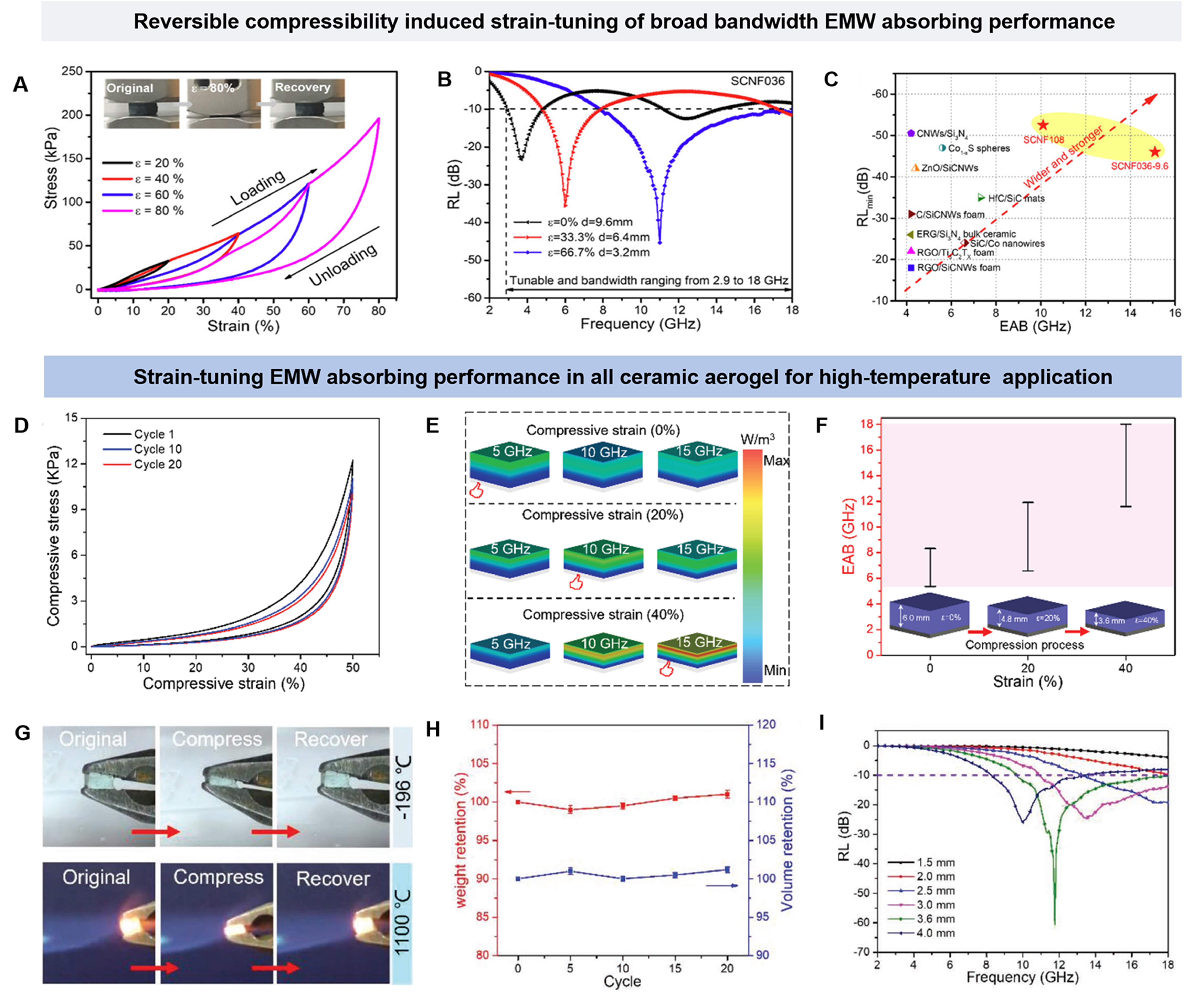
Figure 7. Dynamic absorption frequency tuning enabled by compressible elasticity. (A) Compression-recovery properties, (B) strain-dependent dynamic broadband absorption performance, and (C) comparison of RLmin and EAB with representative EMW absorbing materials for SiC@C nanowire aerogel. (A-C) are reprinted with permission from Ref.[55]. Copyright © 2020, American Chemical Society; (D) Cyclic compression stress-strain curves, (E) simulated power loss density distribution at varying compressive strains, and (F) strain-dependent effective absorption bandwidth of bicontinuous Si3N4/SiC nanowire network; (G) Thermal shock resistance from -196 to
The above experimental observations can be rationalized within the quarter-wavelength matching framework[73], providing a predictive analytical link between compressive strain and the absorption frequency window. For a non-magnetic absorber, the matching condition reads:
where d is the absorber thickness and ε′eff is its effective real permittivity. Under a compressive strain ε, the thickness contracts as d(ε) = d0(1 - ε), while the densification of the network increases the solid volume fraction (1 - P) and thus weakly raises ε′eff according to the effective-medium relation introduced in Section “Compositional optimization for enhancing electromagnetic attenuation” [Equations (1)-(3) and the associated discussion]. Within this approximation, ε′eff varies far more slowly with strain than d does, so that to leading order:
where fm,0 is the matching frequency in the unstrained state. Equation (5) predicts that the matching frequency scales inversely with the residual thickness fraction (1 - ε), establishing a quantitative strain–frequency mapping. Applied to the SCNF discussed above[55], for which fm,0 ≈ 4 GHz at ε = 0, Equation (5) predicts an upshift to ≈ 6 GHz at ε = 33.3% and ≈ 12 GHz at ε = 66.7%, in close agreement with the experimentally observed band-shifting from the C-band to the high end of the Ku-band. This concise analytical relation thus offers a predictive design tool for tailoring strain-tunable EMW absorption in compressible ceramic nanowire aerogels and provides the quantitative basis for the closed-loop adaptive absorber concept discussed in Section “Conclusions and Outlook”.
Extending the strain-tuning strategy to all-ceramic systems, Cai et al. developed an ultralight and resilient bicontinuous Si3N4/SiC nanowire network (BCNCNW) that maintains excellent compressibility and high-temperature stability[52]. The BCNCNW-2 network (Si3N4 content ~44 wt.%, initial density ~8 mg·cm-3, initial thickness 6 mm) exhibits reversible compressibility up to 50% strain with negligible plastic deformation even after 20 compression cycles [Figure 7D]. Under compressive strains of 0%, 20%, and 40%, the average real permittivity (ε′) increases from 3.89 to 3.98 and then to 4.81, while the imaginary permittivity (ε′′) rises from 2.23 to 2.26 and then to 2.74, reflecting the densification of the nanowire network and enhanced conduction loss. Consequently, the EAB of the 6 mm-thick BCNCNW-2 network is continuously adjustable from 5.36 to 18 GHz over the 0%-40% strain range, covering approximately 66% of the C band and the entire X and Ku bands [Figure 7E and F]. Notably, owing to the all-ceramic nature (SiC and Si3N4), the BCNCNW network exhibits exceptional thermal stability up to 1,000 °C in air, thermal shock resistance from -196 to 900 °C [Figure 7G and H], and low thermal conductivity of 32 mW·m-1·K-1. Even after 20 cycles of alternating extreme thermal shocks, the EMW absorption performance remains nearly unchanged [Figure 7I]. This combination of reversible compressibility, strain-tunable broadband absorption, and robust high-temperature tolerance establishes the bicontinuous Si3N4/SiC nanowire aerogel as a compelling platform for adaptive EMW management under extreme service conditions[52].
The strain-tunable absorption strategy pioneered in silicon-based ceramic aerogels has inspired parallel efforts in other material systems. Kong et al. fabricated CNTs/Ti3C2Tx-WPU composite aerogels via bidirectional freeze-drying, achieving deformation-induced absorption band tunability with a minimum reflection loss of -68.2 dB at 42% strain[74]. Wang et al. developed a bio-inspired hyperelastic polydimethylsiloxane (PDMS)-encapsulated aramid NF aerogel with absorption band shifting from C-band to Ku-band under varying strain[75]. Yue et al. reported a superelastic graphene/polyimide fiber composite aerogel delivering an EAB of 12.48 GHz at 4.1 mm thickness, withstanding 90% compressive strain cycles across a -196 to 160 °C temperature window[76]. Beyond mechanical stimuli, Wang et al. prepared CNTs/VO2/ANF composite aerogels leveraging the metal–insulator transition of VO2 to modulate absorption frequency through thermal triggering[77]. However, all these systems are constrained by the limited thermal stability of their polymer or carbon-based matrices, whereas the silicon-based ceramic nanowire aerogels discussed in this review uniquely combine compressible elasticity with high-temperature stability exceeding 1,000 °C, enabling reversible strain-frequency modulation under extreme thermomechanical conditions.
CONCLUSIONS AND OUTLOOK
Addressing the fundamental trade-off between impedance matching and attenuation capacity remains the core scientific issue for advancing high-performance EMW absorbing materials. This review highlights that engineering three-dimensional porous networks from silicon-based ceramic nanowires (SiC and Si3N4) offers a transformative structural solution to decouple this long-standing conflict.
The ultrahigh porosity (> 90%) of these aerogels effectively reduces the effective permittivity toward that of free space, directly improving impedance matching. Simultaneously, the interconnected nanowire architecture provides abundant heterogeneous interfaces (e.g., SiC@C core-shell[55], SiC/SiO2[57], SiC/Si3N4[47,52]), stacking-fault-induced dipole centers, and continuous conductive pathways, enabling multi-scale polarization and resistive dissipation. By incorporating conductive carbon coatings or magnetic Ni nanoparticles, dielectric and magnetic losses are further enhanced[50,55]. Introducing a low-dielectric wave-transparent Si3N4 phase or an amorphous SiO2 sheath allows precise impedance gradient optimization, yielding broadband high-temperature absorption up to 1,000 °C. Moreover, the compressible elasticity (reversible strain up to 80%) of these all-ceramic aerogels uniquely enables dynamic, strain-tunable absorption frequency bands-a capability previously limited to carbon-based systems but now realized in thermally robust ceramics.
Despite these advances, several limitations remain. First, most reported performances are based on laboratory-scale synthesis; scalable, cost-effective manufacturing routes are lacking. Second, the long-term cyclic mechanical stability and oxidation resistance of flexible ceramic aerogels under extreme thermomechanical conditions require further validation. Third, the integration of magnetic loss components that retain high-temperature stability (e.g., high-Curie-temperature magnetic ceramics) remains underexplored. Finally, the relationship between macroscopic mechanical deformation and microscopic EM response is still largely empirical, lacking predictive models.
To address these challenges and accelerate the practical deployment of silicon-based ceramic nanowire aerogels, the following five research directions are proposed.
(1) Decoupling impedance-attenuation trade-offs via programmable multi-scale architectures. Hierarchically structured aerogels with independently tailored macro-scale lattice periodicity, meso-scale porosity gradients, and nano-scale core-shell interfaces are needed to push absorption toward the full 2-18 GHz range. The main barrier is the resolution gap between ceramic 3D printing (50 to 100 μm) and the nanowire scale (~50 nm), compounded by the incompatibility of > 1,300 °C CVD with most polymer-based templates. A practical near-term route is two-step manufacturing, in which mesoscale lattices are printed first and then populated with nanowires via subsequent CVD, accelerated by genetic-algorithm-assisted gradient design as already demonstrated in SiC@SiO2 systems.
(2) Intelligent adaptive absorbers with closed-loop strain-frequency control. Building on the analytical relation in Section “Strain-Driven Dynamic Modulation of Broadband Electromagnetic Wave Absorption” [Equation (5)], integrated actuator-sensor-absorber platforms could autonomously match dynamic EM environments by adjusting density and thickness. The main bottleneck is that piezoelectric and shape-memory drivers degrade above 500 °C, and existing high-temperature strain sensors are not compatible with brittle ceramic aerogels. Near-term efforts should therefore focus on offline machine-learning surrogates trained on strain-permittivity datasets, with on-board closed-loop control awaiting compatible high-temperature actuators.
(3) High-temperature multifunctional integration centered on EMW absorption. The same 3D ceramic network can co-deliver wave absorption and complementary functions for hypersonic radomes, re-entry capsules, and high-temperature radar-absorbing structures. The main conflict is that high porosity favors impedance matching but compromises load-bearing capability and ablation resistance. Gradient or hybrid architectures featuring a dense outer skin and a porous absorbing core, designed via finite-element-aided trade-off mapping, offer a realistic compromise.
(4) Scalable and cost-effective manufacturing routes. Continuous, low-cost processes such as ambient-pressure drying, roll-to-roll nanowire assembly, and freeze-casting must be developed without sacrificing porosity above 90% or nanowire aspect ratio. Supercritical drying preserves structural integrity but is energy-intensive (> 10 MPa) and difficult to scale, whereas ambient-pressure drying typically causes > 30% volumetric shrinkage and consequent permittivity drift. Freeze-casting and surface-modification-assisted ambient drying are realistic candidates for pilot-scale production within 5 to 10 years, provided that nanowire connectivity and impurity content are tightly controlled.
(5) Synergistic magnetic–dielectric–wave-transparent tri-phase systems for high-temperature operation. All-ceramic tri-network architectures incorporating high-Curie-temperature magnetic ceramics into SiC/Si3N4 aerogels could overcome the Snoek limit and extend broadband absorption to 800 to 1,000 °C, building on the SiC/Ni@CMT concept. The challenge is that conventional ferrites lose magnetism above 300 to 600 °C, whereas high-Curie-temperature alternatives such as M-type hexaferrites or Fe-based intermetallics are difficult to incorporate without disrupting nanowire connectivity. In situ growth of magnetic nanoparticles at nanowire junctions, with rare-earth-doped hexaferrites (Curie temperature above 700 °C) as the most promising candidate, offers a viable route.
(6) Long-term EM stability under sustained service. Most current studies report only initial-state performance, leaving the evolution of EMW response under prolonged high-temperature exposure or repeated strain cycling poorly characterized. Progressive SiO2 sheath thickening on SiC nanowires, as evidenced in controlled-oxidation studies, increases inter-nanowire tunneling distance and shifts the matching frequency, indicating that service-life stability is governed by interface evolution rather than by initial composition. Standardized accelerated aging combined with periodic complex permittivity characterization is needed to establish empirical degradation laws and to feed predictive service-life models.
In summary, silicon-based ceramic nanowire aerogels represent a paradigm shift from conventional bulk or powder absorbers. With continued advances in hierarchical design, adaptive control, multifunctional integration, scalable manufacturing, and high-temperature magnetic-dielectric synergy, these materials hold great promise for next-generation flexible EMW absorption in extreme environments.
DECLARATIONS
Authors’ contributions
Conceptualization: Su, L.; Wang, H.
Writing: Su, L.; Wu, W.; Dang C.
Validation, resources: Su, L.; Wu, W.
Review and editing, supervision, project administration: Wang, H.; Dang, C.; Cai, Z.; Ni, Z.
Funding acquisition: Wang, H.; Su, L.
Availability of data and materials
Not applicable.
AI and AI-assisted tools statement
Not applicable.
Financial support and sponsorship
This work is supported by the National Natural Science Foundation of China (No. 52572083, 92263204, 52102076), the Fundamental Research Funds for the Central Universities, and the Top Young Talents Program of Xi’an Jiaotong University.
Conflicts of interest
All authors declared that there are no conflicts of interest.
Ethical approval and consent to participate
Not applicable.
Consent for publication
Not applicable.
Copyright
© The Author(s) 2026.
REFERENCES
1. Wang, X. X.; Cao, W. Q.; Cao, M. S.; Yuan, J. Assembling nano-microarchitecture for electromagnetic absorbers and smart devices. Adv. Mater. 2020, 32, e2002112.
2. Iqbal, A.; Shahzad, F.; Hantanasirisakul, K.; et al. Anomalous absorption of electromagnetic waves by 2D transition metal carbonitride Ti3CNTx (MXene). Science 2020, 369, 446-50.
3. Shahzad, F.; Alhabeb, M.; Hatter, C. B.; et al. Electromagnetic interference shielding with 2D transition metal carbides (MXenes). Science 2016, 353, 1137-40.
4. Quan, B.; Liang, X.; Ji, G.; et al. Dielectric polarization in electromagnetic wave absorption: review and perspective. J. Alloys. Compd. 2017, 728, 1065-75.
5. Qin, M.; Zhang, L.; Wu, H. Dielectric loss mechanism in electromagnetic wave absorbing materials. Adv. Sci. 2022, 9, e2105553.
6. Jin, H.; Liu, M.; Wang, L.; et al. Design and fabrication of 1D nanomaterials for electromagnetic wave absorption. Natl. Sci. Rev. 2025, 12, nwae420.
7. Hou, Z.; Gao, X.; Zhang, J.; Wang, G. A perspective on impedance matching and resonance absorption mechanism for electromagnetic wave absorbing. Carbon 2024, 222, 118935.
8. Narang, S. B.; Pubby, K. Nickel spinel ferrites: a review. J. Magn. Magn. Mater. 2021, 519, 167163.
9. Özgür, Ü.; Alivov, Y.; Morkoç, H. Microwave ferrites, part 1: fundamental properties. J. Mater. Sci. Mater. Electron. 2009, 20, 789-834.
10. Zheng, W.; Ye, W.; Yang, P.; et al. Recent progress in iron-based microwave absorbing composites: a review and prospective. Molecules 2022, 27, 4117.
11. Song, Q.; Ye, F.; Kong, L.; et al. Graphene and MXene nanomaterials: toward high‐performance electromagnetic wave absorption in gigahertz band range. Adv. Funct. Mater. 2020, 30, 2000475.
12. Cao, M.; Wang, X.; Zhang, M.; et al. Electromagnetic response and energy conversion for functions and devices in low‐dimensional materials. Adv. Funct. Mater. 2019, 29, 1807398.
13. Che, R.; Peng, L.; Duan, X.; Chen, Q.; Liang, X. Microwave absorption enhancement and complex permittivity and permeability of Fe encapsulated within carbon nanotubes. Adv. Mater. 2004, 16, 401-5.
14. Lv, H.; Yang, Z.; Pan, H.; Wu, R. Electromagnetic absorption materials: current progress and new frontiers. Prog. Mater. Sci. 2022, 127, 100946.
15. Liang, L.; Li, Q.; Yan, X.; et al. Multifunctional magnetic Ti3C2Tx MXene/graphene aerogel with superior electromagnetic wave absorption performance. ACS. Nano. 2021, 15, 6622-32.
16. Kim, S. H.; Lee, S. Y.; Zhang, Y.; Park, S. J.; Gu, J. Carbon-based radar absorbing materials toward stealth technologies. Adv. Sci. 2023, 10, e2303104.
17. Wu, Y.; Tan, S.; Fang, G.; Zhang, Y.; Ji, G. Manipulating CNT films with atomic precision for absorption effectiveness–enhanced electromagnetic interference shielding and adaptive infrared camouflage. Adv. Funct. Mater. 2025, 35, 2402193.
18. Wang, Z. Y.; Li, Z. C.; Li, B.; et al. Functional carbon springs enabled dynamic tunable microwave absorption and thermal insulation. Adv. Mater. 2024, 36, e2412605.
19. Wang, T.; Zhao, W.; Miao, Y.; et al. Enhancing defect-induced dipole polarization strategy of SiC@MoO3 nanocomposite towards electromagnetic wave absorption. Nanomicro. Lett. 2024, 16, 273.
20. Kuang, J.; Cao, W. Stacking faults induced high dielectric permittivity of SiC wires. Appl. Phys. Lett. 2013, 103, 112906.
21. Weng, W.; Wang, S.; Xiao, W.; Lou, X. W. D. Direct conversion of rice husks to nanostructured SiC/C for CO2 photoreduction. Adv. Mater. 2020, 32, e2001560.
22. Su, L.; Wang, H.; Niu, M.; et al. Ultralight, recoverable, and high-temperature-resistant SiC nanowire aerogel. ACS. Nano. 2018, 12, 3103-11.
23. Shen, Z.; Chen, J.; Li, B.; Li, G.; Zhang, Z.; Hou, X. Recent progress in SiC nanowires as electromagnetic microwaves absorbing materials. J. Alloys. Compd. 2020, 815, 152388.
24. Jiang, J.; Yan, L.; Xue, Y.; et al. Lightweight and thermally insulating polymer-derived SiBCN/SiCnw ceramic aerogel with enhanced electromagnetic wave absorbing performance. Chem. Eng. J. 2024, 482, 148878.
25. Niu, M.; Wang, H.; Su, L.; et al. Lightweight and resilient SiOC/SiC foam with efficient electromagnetic wave absorption and high‐temperature stability. J. Am. Ceram. Soc. 2023, 106, 3078-88.
26. Wang, K.; Chu, W.; Liu, X.; Li, X.; Liu, H. Recent advances in carbon-based microwave-absorbing aerogel. Soft. Sci. 2026, 6, 8.
27. Zhou, M.; Yu, Z.; Yan, Q.; Zhang, X. Asymmetric structural design for absorption‐dominated electromagnetic interference shielding composites. Adv. Funct. Mater. 2025, 35, 2423884.
28. Su, R.; Liu, P.; Chen, J.; et al. Self‐assembly and 3D printing of SiCw@MXene/SiOC metastructure toward simultaneously excellent terahertz electromagnetic interference (EMI) shielding and electron‐to‐thermal conversion properties. Adv. Funct. Mater. 2025, 35, 2500970.
29. Zeng, X.; Wu, L.; Yang, X.; et al. Design of gel‐based materials for electromagnetic wave absorption. Adv. Funct. Mater. 2025, 35, 2502671.
30. Guo, R.; Zheng, Q.; Wang, L.; Fan, Y.; Jiang, W. Porous N-doped Ni@SiO2/graphene network: three-dimensional hierarchical architecture for strong and broad electromagnetic wave absorption. J. Mater. Sci. Technol. 2022, 106, 108-17.
31. Han, M.; Yin, X.; Hou, Z.; et al. Flexible and thermostable graphene/SiC nanowire foam composites with tunable electromagnetic wave absorption properties. ACS. Appl. Mater. Interfaces. 2017, 9, 11803-10.
32. Zhao, W.; Shao, G.; Jiang, M.; et al. Ultralight polymer-derived ceramic aerogels with wide bandwidth and effective electromagnetic absorption properties. J. Eur. Ceram. Soc. 2017, 37, 3973-80.
33. Qiao, M.; Lei, X.; Ma, Y.; et al. Application of yolk–shell Fe3O4@N-doped carbon nanochains as highly effective microwave-absorption material. Nano. Res. 2018, 11, 1500-19.
34. Huang, B.; Ye, F.; Deng, J.; et al. Cross-scale structural engineering of MOF-derived CoxNiy@C nanorods with controllable electromagnetic response behavior for broadband electromagnetic wave absorption. J. Adv. Ceram. 2026, 15, 9221224.
35. Zhang, Y.; Huang, Y.; Zhang, T.; et al. Broadband and tunable high-performance microwave absorption of an ultralight and highly compressible graphene foam. Adv. Mater. 2015, 27, 2049-53.
36. Wang, Z.; Wei, R.; Gu, J.; et al. Ultralight, highly compressible and fire-retardant graphene aerogel with self-adjustable electromagnetic wave absorption. Carbon 2018, 139, 1126-35.
37. Zhan, B.; Qu, Y.; Qi, X.; et al. Mixed-dimensional assembly strategy to construct reduced graphene oxide/carbon foams heterostructures for microwave absorption, anti-corrosion and thermal insulation. Nanomicro. Lett. 2024, 16, 221.
38. Zhao, H.; Zhang, C.; Li, Y.; et al. Ordered cellular 2D/2D biomass-derived carbon nanosheet/MXene aerogels for ultralight and high-performance microwave absorption. J. Adv. Ceram. 2025, 14, 9221214.
39. Zhang, Y.; Li, S.; Tang, X.; et al. Ultralight and ordered lamellar polyimide-based graphene foams with efficient broadband electromagnetic absorption. J. Mater. Sci. Technol. 2022, 102, 97-104.
40. Chen, G.; Li, Z.; Zhang, L.; et al. Mechanisms, design, and fabrication strategies for emerging electromagnetic wave-absorbing materials. Cell. Rep. Phys. Sci. 2024, 5, 102097.
41. Li, C.; Li, D.; Zhang, S.; et al. Interface engineering of titanium nitride nanotube composites for excellent microwave absorption at elevated temperature. Nanomicro. Lett. 2024, 16, 168.
42. Wang, Q.; Qi, L.; Jia, Y.; Li, H. Flexible ZrO2/ZrC/ZrB2 ceramic nanofiber mats by electrospinning with broadband electromagnetic absorption and high-temperature oxidation resistance. Mater. Lett. 2024, 365, 136442.
43. Zhang, Y.; Li, R.; Luo, W.; et al. High‐efficiency electromagnetic absorption of HfC–SiCf ceramics with a 3D reticular structure. J. Am. Ceram. Soc. 2025, 108, e20213.
44. Hao, B.; Chai, Z.; Li, M.; et al. Design of mesoscopic metacomposites for electromagnetic wave absorption: enhancing performance and gaining mechanistic insights. Soft. Sci. 2025, 5, 39.
45. Si, H.; Zhang, S.; Ding, Y.; et al. Enhanced microwave trapping and loss capabilities of TiN/RGO/PDMS metacomposites across a wide range of temperatures. Research 2025, 8, 0972.
46. Zhang, H.; Xu, Y.; Zhou, J.; et al. Stacking fault and unoccupied densities of state dependence of electromagnetic wave absorption in SiC nanowires. J. Mater. Chem. C. 2015, 3, 4416-23.
47. Wang, L.; Cai, Z.; Su, L.; et al. Bifunctional SiC/Si3N4 aerogel for highly efficient electromagnetic wave absorption and thermal insulation. J. Adv. Ceram. 2023, 12, 309-20.
48. Dai, D.; Lan, X.; Wu, L.; Wang, Z. Designed fabrication of lightweight SiC/Si3N4 aerogels for enhanced electromagnetic wave absorption and thermal insulation. J. Alloys. Compd. 2022, 901, 163651.
49. Geng, W.; Song, L.; Liu, Y.; et al. Air layer-engineered Cf@void@SiCnf composites for enhanced electromagnetic wave absorption. Chem. Eng. J. 2025, 524, 169149.
50. Cai, Z.; Su, L.; Wang, H.; et al. Hierarchically assembled carbon microtube@SiC nanowire/Ni nanoparticle aerogel for highly efficient electromagnetic wave absorption and multifunction. Carbon 2022, 191, 227-35.
51. Ni, Z.; Lu, D.; Jia, S.; et al. Gradient impedance all-ceramic aerogels: resolving the trade-off between broadband and strong microwave absorption. ACS. Appl. Mater. Interfaces. 2025, 17, 43189-98.
52. Cai, Z.; Su, L.; Niu, M.; et al. Ultralight and resilient bicontinuous Si3N4/SiC nanowire network for tunable and highly efficient electromagnetic wave absorption in extreme conditions. Adv. Mater. Interfaces. 2022, 9, 2201553.
53. Zhang, B.; Zhi, W.; Duan, J.; Zhang, L.; Liang, F.; Ma, C. Mechanically robust SiC aerogel with both electromagnetic absorption and pollutant adsorption via microtube/nanowire structure design. J. Adv. Ceram. 2025, 14, 9221181.
54. Pozar, D. M. Microwave engineering, 4th edition. John wiley & sons; 2011. https://www.wiley.com/en-us/Microwave+Engineering%2C+4th+Edition-p-9780470631553. (accessed 2026-07-08).
55. Cai, Z.; Su, L.; Wang, H.; et al. Hydrophobic SiC@C nanowire foam with broad-band and mechanically controlled electromagnetic wave absorption. ACS. Appl. Mater. Interfaces. 2020, 12, 8555-62.
56. Song, M.; Yan, L.; Li, Y.; et al. Thermal insulated C/SiC nanofiber aerogel with high thermal stability and superior electromagnetic wave absorption performance. Ceram. Int. 2024, 50, 28907-17.
57. Wang, Z.; Liu, J.; Hao, H.; et al. Microwave absorption enhancement by SiC nanowire aerogels through heat treatment-based oxidation modulation. Carbon 2024, 217, 118622.
58. Chen, Y.; Peng, H.; Cai, B.; et al. Synthesis of ultralight hollow SiC/C nanofiber for highly efficient electromagnetic wave absorption. J. Adv. Ceram. 2026, 15, 9221225.
59. Yuan, K.; Han, D.; Liang, J.; et al. Microwave induced in-situ formation of SiC nanowires on SiCNO ceramic aerogels with excellent electromagnetic wave absorption performance. J. Adv. Ceram. 2021, 10, 1140-51.
60. Guo, P.; Su, L.; Jia, S.; et al. Strong SiC@carbon nanowire aerogel metamaterials for efficient electromagnetic interference shielding. Carbon 2024, 229, 119492.
61. You, X.; Ouyang, H.; Deng, R.; et al. Graphene aerogel composites with self-organized nanowires-packed honeycomb structure for highly efficient electromagnetic wave absorption. Nanomicro. Lett. 2024, 17, 47.
62. Yu, G.; Shao, G.; Xu, Z.; Chen, Y.; Huang, X. Hierarchical interface-engineered magnetic graphene‒SiCN aerogels via a stepwise confinement strategy for low-frequency and broadband microwave absorption. J. Adv. Ceram. 2025, 14, 9221187.
63. Jiang, J.; Yan, L.; Song, M.; et al. Thermally insulated C/SiC/SiBCN composite ceramic aerogel with enhanced electromagnetic wave absorption performance. Ceram. Int. 2025, 51, 17-24.
64. Zhang, W.; Su, L.; Lu, D.; et al. Resilient Si3N4@SiO2 nanowire aerogels for high-temperature electromagnetic wave transparency and thermal insulation. J. Adv. Ceram. 2023, 12, 2112-22.
65. Cai, Z.; Su, L.; Wang, H.; et al. Alternating multilayered Si3N4/SiC aerogels for broadband and high-temperature electromagnetic wave absorption up to 1000 °C. ACS. Appl. Mater. Interfaces. 2021, 13, 16704-12.
66. Wang, Q.; Wang, G.; Lu, X.; Su, L.; Wang, H. Prediction of broadband and highly-efficient electromagnetic wave-absorbing SiC@SiO2 nanowire aerogel by genetic algorithm. ACS. Appl. Mater. Interfaces. 2024, 16, 57972-80.
67. Jiang, J.; Yan, L.; Li, J.; et al. Lightweight, thermally insulating SiBCN/Al2O3 ceramic aerogel with enhanced high-temperature resistance and electromagnetic wave absorption performance. Chem. Eng. J. 2024, 501, 157656.
68. Yan, M.; Pan, Y.; He, P.; et al. Mechanically strong SiC aerogels with broadband electromagnetic wave absorption enabled by hollow skeleton and interface engineering. Chem. Eng. J. 2024, 497, 154556.
69. Wang, X.; Chen, X.; He, Q.; et al. Bidirectional, multilayer MXene/polyimide aerogels for ultra-broadband microwave absorption. Adv. Mater. 2024, 36, e2401733.
70. Wang, X.; Yuan, Y.; Wang, L.; et al. Intelligent design of multifunctional graphene-based aerogels for ultra-broadband microwave absorption. J. Adv. Ceram. 2025, 14, 9221172.
71. Liu, C.; Mao, K.; Sun, H.; et al. Integrated design of multifunctional paraffin-impregnated porous ceramic metastructures for electromagnetic wave absorption and thermal management. J. Adv. Ceram. 2025, 14, 9221155.
72. Wang, J.; Li, Y.; Cao, J.; et al. Robust and thermally insulating SiBCN/SiOC ceramic aerogel with superior electromagnetic wave absorption performance and high-temperature stability up to 1600 °C. J. Adv. Ceram. 2026, 15, 9221256.
74. Kong, L.; Zhang, G.; Cui, H.; Qi, J.; Wang, T.; Xu, H. Deformation induced absorption band-tunable smart CNTs/Ti3C2Tx-WPU electromagnetic wave absorbing aerogel. Carbon 2024, 223, 119023.
75. Wang, C.; Yang, J.; Hu, C.; et al. Flexible bamboo-based microcapacitance-schottky heterostructures for integrated microwave absorption and self-powered wearable sensing. Adv. Compos. Hybrid. Mater. 2026, 9, 1567.
76. Yue, J.; Qin, M.; Yu, H.; He, Q.; Feng, W. Superelastic graphene‐based composite aerogel for thermal and electromagnetic protection in extreme temperature environments. Adv. Funct. Mater. 2025, 35, 2508319.
Cite This Article
 Open Access
How to Cite
Download Citation
Export Citation File:
Type of Import
Tips on Downloading Citation
Citation Manager File Format
Type of Import
Direct Import: When the Direct Import option is selected (the default state), a dialogue box will give you the option to Save or Open the downloaded citation data. Choosing Open will either launch your citation manager or give you a choice of applications with which to use the metadata. The Save option saves the file locally for later use.
Indirect Import: When the Indirect Import option is selected, the metadata is displayed and may be copied and pasted as needed.
About This Article
Special Topic
Copyright

Data & Comments
Data
0








Comments
Comments must be written in English. Spam, offensive content, impersonation, and private information will not be permitted. If any comment is reported and identified as inappropriate content by OAE staff, the comment will be removed without notice. If you have any queries or need any help, please contact us at support@oaepublish.com.