




fig2
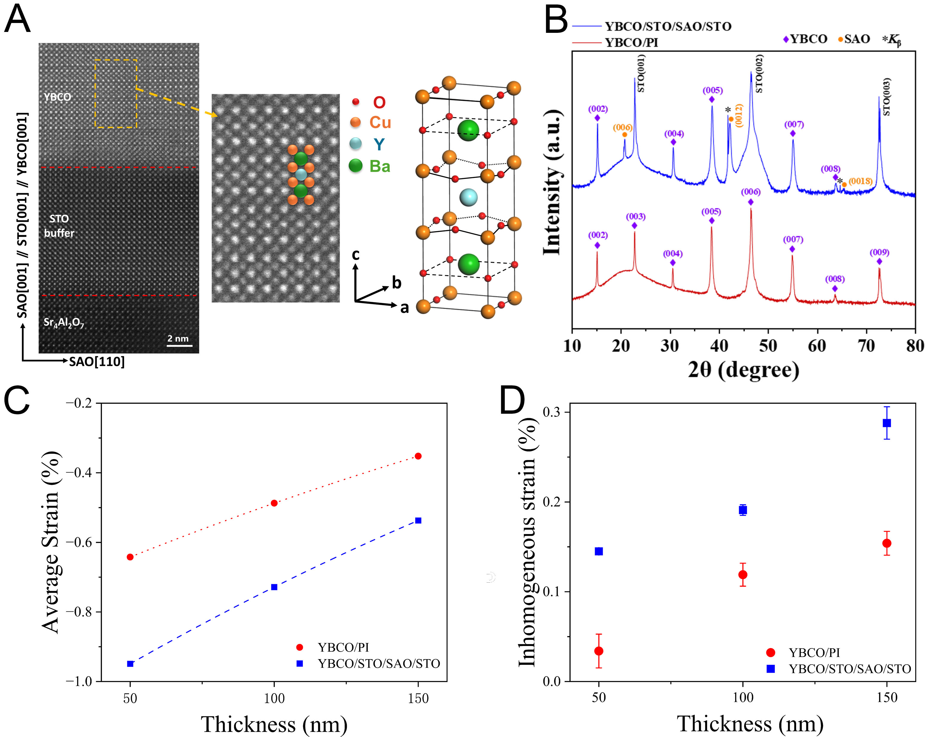
Figure 2. (A) Cross-sectional HAADF-STEM images of YBCO/STO/SAO structure. On the right is an enlarged view of the orange rectangle-enclosed region and a schematic diagram of the YBCO crystal structure; (B) XRD comparison of YBCO thin film before and after peeling and its corresponding structural diagram. Before peeling (blue), the YBCO (003), (006), and (009) diffraction peaks overlap with the STO (001), (002), and (003) peaks. After peeling (red), the YBCO (002) to (009) diffraction peaks are clearly visible; (C) Average out-of-plane strain as a function of thickness; (D) Inhomogeneous strain as a function of film thickness for different structures. The error bars originate from the standard error of the slope. YBCO: YBa2Cu3O7; STO: SrTiO3; SAO: Sr4Al2O7; HAADF-STEM: high-angle annular dark-field scanning transmission electron microscopy; XRD: X-ray diffraction.