




Strain-modulation and enhancement of superconductivity in flexible YBa2Cu3O7 thin films
 0
0 Abstract
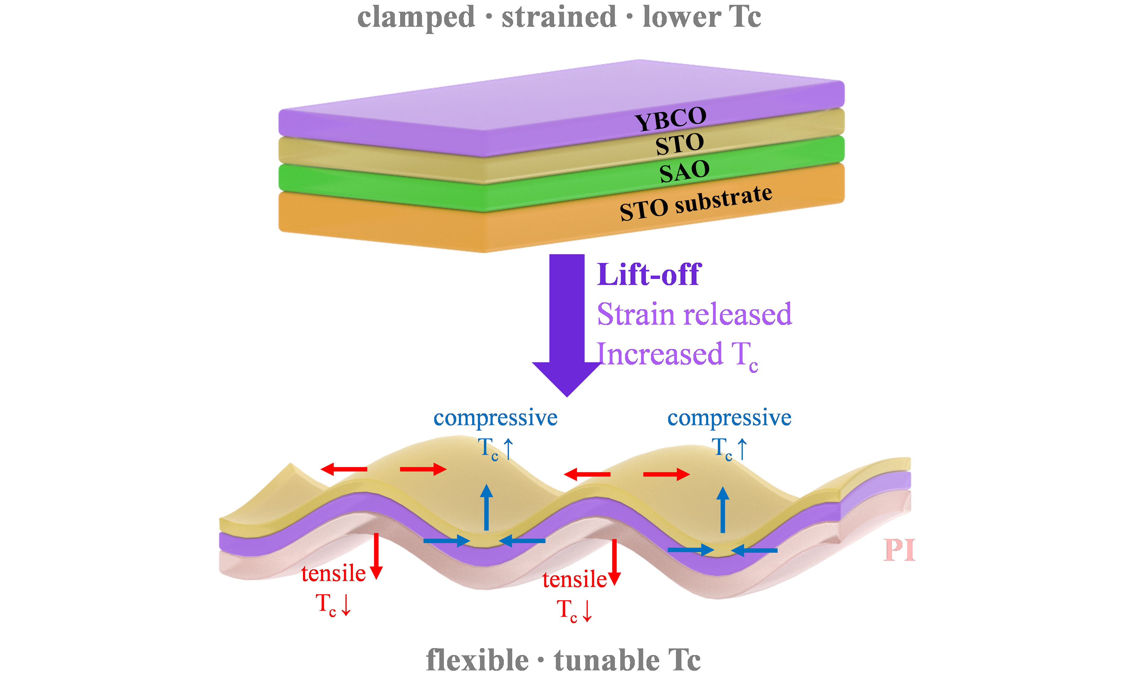
The development of large, high-quality flexible high-temperature superconducting films is a crucial focus in flexible electronics research, posing challenges and offering promising applications. Among candidate materials, YBCO is a high-performance high-temperature superconductor. However, the mechanical behavior and stress evolution of its flexible thin films remain a critical gap in current research, hindering further development. In this investigation, a YBa2Cu3O7/SrTiO3/Sr4Al2O7 heterostructure was synthesized on SrTiO3 substrates via pulsed laser deposition (PLD). By selectively etching the water-soluble Sr4Al2O7 sacrificial layer, crack-free, high-quality freestanding YBa2Cu3O7 films at the millimeter scale were successfully fabricated, and remarkable improvements in superconducting properties were achieved, with critical transition temperature and magnetic shielding response approaching the intrinsic characteristics of bulk YBa2Cu3O7. Bending experiments demonstrate that the superconductivity of freestanding YBCO films can be effectively modulated by mechanical strain. Under in‑plane compressive strain, the film exhibits an increased superconducting transition temperature, whereas in‑plane tensile strain diminishes superconductivity. This study not only presents a dependable approach for producing high-quality flexible high-temperature superconducting films but also establishes a fundamental strain-modulation mechanism. By controlling bending, achieved enhancement and continuous modulation of the superconducting properties. These results are essential for the advancement of new-generation flexible electronic devices based on high-temperature superconducting materials.
Keywords
INTRODUCTION
The high-temperature superconducting material yttrium barium copper oxide (YBa2Cu3O7-δ, YBCO) has demonstrated considerable application potential in the field of industrial superconductivity due to its outstanding superconducting properties (critical temperature Tc > 90 K) and high critical current density (Jc)[1]. However, conventional rigid YBCO films face substantial limitations in applications involving flexible electronic devices, wearable superconducting devices, and multifunctional integrated systems. In recent years, van der Waals two-dimensional nanomaterials have spurred many exciting advances in both fundamental research and practical applications. Their unique advantages in material design and performance tuning have repeatedly had a profound impact on science and technology[2-5]. In the field of complex oxides, the rich electronic states, magnetic properties, and mechanical behavior exhibited by epitaxial films and their interfaces have established this area as an essential research direction in condensed matter physics and functional materials[6-11]. Inspired by two-dimensional van der Waals materials, the oxide thin film community has made a series of major breakthroughs in fabricating complex oxide heterostructures[12-15]. For instance, recent demonstration of field-free, reversible Josephson diode effects in artificially stacked Bi2Sr2CaCu2O8-x heterostructures by controlling the stacking angle[16]. This phenomenon displays a technologically analogous mechanism to the twist-angle-dependent effects observed in magic-angle graphene systems[17-19].
The combination of YBCO superconducting layers with flexible substrates opens new approaches for flexible quantum technologies, where the realization of macroscopic freestanding YBCO membranes with preserved superconducting properties could enable unprecedented device architecture. In 1994, Wu et al.[20] pointed out the critical role of textured buffer layers in preserving both film quality and mechanical flexibility in YBCO systems. Subsequent studies have systematically demonstrated that multilayer architectures can notably enhance the functional characteristics of YBCO films through interface engineering[21-24]. Li et al.[25] emphasized the importance of interfacial lattice matching for optimizing both microstructural properties and superconducting performance parameters. In recent years, researchers have reported more experiments for self-supporting oxide thin films, confirming that these fabrication processes can maintain high crystallinity and electronic quality, as evidenced by high-resolution transmission electron microscopy and angle-resolved photoemission spectroscopy measurements[26-28]. To overcome the challenges of aqueous sensitivity and buffer layer requirements of YBCO thin films, Jia et al.[29] proposed a buffer-layer-free transfer method for transferring YBCO films to flexible substrates, facilitating the development of self-supporting flexible superconducting films.
From optimizing epitaxial growth to enhancing functional properties through multilayer structures, and to developing transfer techniques, these research achievements highlight the importance of microstructural properties, buffer layer engineering, and innovative transfer methods in advancing the development of YBCO flexible thin film technology. However, systematic research of the mechanical behavior and stress evolution mechanisms of YBCO flexible films during preparation and transfer remains limited. This research gap stems largely from the formation of cracks and wrinkles during fabrication[30], which lead to localized strain relaxation and macroscopic inhomogeneity, thereby making it difficult to assess the mechanical properties and stress variation of large-area films. As flexible electronics progress toward practical applications, understanding the mechanical evolution and its correlation with changes in physical properties becomes indispensable. Therefore, investigating the mechanical behavior of YBCO flexible films during preparation and its impact on superconducting properties represents an urgent scientific challenge. To address this gap, we propose a novel thin-film fabrication transfer strategy based on a water-soluble sacrificial layer[31] and apply it to YBCO thin films. The water-soluble sacrificial layer Sr3Al2O6 has been established as a robust and universal approach for thin film transfer[32]. Remarkably, Zhang et al.[33] recently discovered a previously unreported Sr4Al2O7 phase which exhibits excellent structural flexibility and high water solubility, substantially improving the size and quality of thin film lift-off.
Here, we report a fabrication method for freestanding YBCO thin films by selectively etching the water-soluble sacrificial layer Sr4Al2O7 (the following is simply referred to as SAO). Structural characterization and transport measurements confirm the reliability of this method, which yields high-quality, crack-free YBCO freestanding thin films with dimensions nearly as large as the substrate (5 mm × 5 mm), and interestingly, its superconducting properties exhibit a pronounced enhancement. This optimization can be attributed to the lift-off process, which releases the in-plane tensile strain caused by lattice mismatch during the growth. This fabrication methodology and its strain-release mechanism are highly universal and can be extended to the synthesis and processing of freestanding thin films in different materials, thereby providing valuable references for strain-gradient engineering in other systems, such as flexible ferroelectric, ferromagnetic, and related functional thin films. These high-quality freestanding films enable further investigation of the effect of strain engineering on the superconductivity of flexible YBCO. Our experimental results indicate that strain can continuously adjust superconductivity in flexible YBCO films. These results not only provide an experimental foundation for exploring the superconducting mechanism of high-temperature cuprates but also open new avenues for flexible electronic systems and practical applications.
MATERIALS AND METHODS
Preparation of YBCO/STO/SAO/STO heterostructure thin films
In this study, high-quality epitaxial YBa2Cu3O7 (YBCO) films with varying thicknesses were grown on single-crystal SrTiO3 (STO) substrates using pulsed laser deposition (PLD, Twente Solid State Technology-CUSTOMIZED, Netherlands). To facilitate subsequent lift-off processes, the highly water-soluble Sr4Al2O7 (SAO) was selected as the sacrificial layer. Additionally, a 10-nm-thick SrTiO3 buffer layer was grown between the YBCO film and SAO layer to prevent potential aqueous corrosion damage to the YBCO film during the lift-off procedure. Specifically, single-side-polished STO (001) substrates with dimensions of 5 mm × 5 mm × 0.5 mm were selected for epitaxial film growth. The single-crystalline oxide films were deposited via pulsed-laser deposition (PLD) using a 248 nm KrF excimer laser (Lambda Physik COMPex 205, Germany). Initially, a 40 nm-thick SAO layer was grown at 750 °C under an oxygen pressure of 0.01 mbar, employing the laser energy density of 1 J/cm2 at a repetition rate of 3 Hz. Through in situ target exchange while maintaining the same temperature and oxygen pressure environment, a 10 nm-thick STO buffer layer was epitaxially deposited using a laser energy density of 1 J/cm2 at 2 Hz. Subsequently, the oxygen pressure was increased to 0.35 mbar, the substrate temperature was kept at 750 °C, and YBCO layers with thicknesses of 50 nm, 100 nm, and 150 nm were epitaxially deposited using laser energy densities of 2 J/cm2 and a repetition rate of 1 Hz. Finally, the sample was annealed at 1000 mbar oxygen pressure and cooled to room temperature at a rate of 10 °C/min.
Flexible film fabrication
Figure 1A shows a schematic diagram of the entire peeling process. Following film growth, a polyimide (PI) layer was adhered to the YBCO surface using M-Bond 610 adhesive. This configuration serves dual purposes: first, to ensure robust mechanical support during the lift-off process; and second, it protects the YBCO film from potential damage during etching. The M-Bond 610 (TED PELLA) adhesive adjusts the volume ratio of the “curing agent” and “adhesive” to 3:4 (slightly reducing the content of the curing agent compared to the standard formulation). This adjusted composition yielded a more compliant bonding layer, which facilitated enhanced stress release during the peeling process. The sample was then placed on a temperature-controlled hotplate at 60 °C for 24 h to ensure complete polymerization and stabilization of the M-Bond adhesive. The sacrificial Sr4Al2O7 (SAO) layer was selectively etched by immersing the entire heterostructure in deionized water, leading to its complete dissolution and the release of the YBCO film from the SrTiO3 substrate (as shown in Figure 1B). This process yielded large-size, crack-free freestanding YBCO single-crystalline films with exceptional structural integrity, as confirmed by optical microscopy (Figure 1C and also as shown in Supplementary Figure 1). The resulting freestanding films exhibit great crystallinity and mechanical robustness, making them suitable for further characterization and measurements.
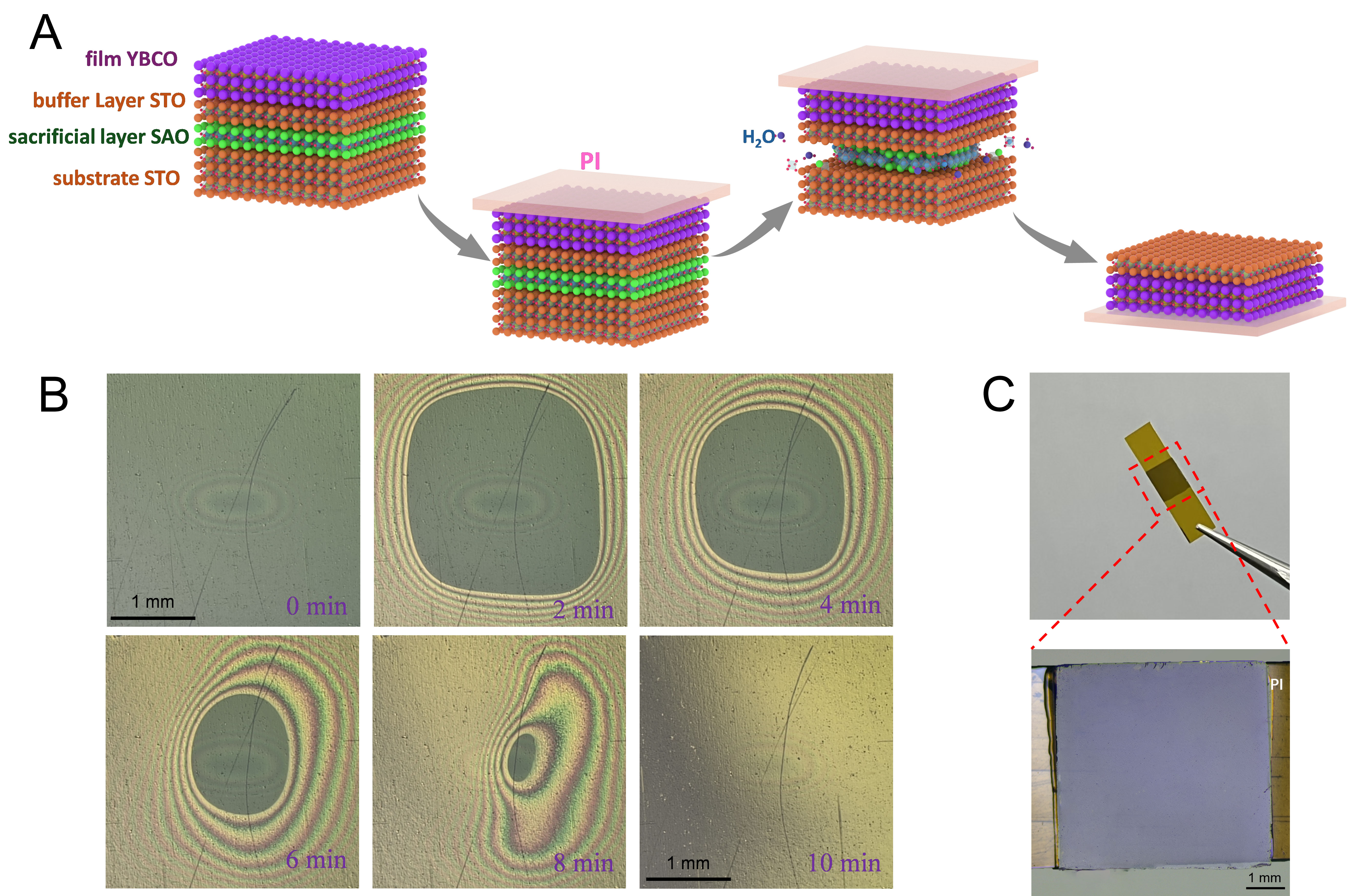
Figure 1. (A) Schematic diagram of the peeling process; (B) Top-view images of the sample during the dissolution process over time within a 3 mm × 3 mm area, illustrating the continuous and uniform diffusion of the dissolved region from the periphery toward the central zone; (C) Photos of YBCO thin film samples after peeling. The film size after peeling remains almost the same, with integrity and no cracks. YBCO: YBa2Cu3O7.
RESULTS AND DISCUSSIONS
Structural characterization and analysis
Cross-sectional high-angle annular dark-field scanning transmission electron microscopy (HAADF-STEM, Thermo Scientific Talos F200S, USA) imaging of the YBCO/STO/SAO/STO heterostructure [Figure 2A] reveals well-defined epitaxial interfaces at both the bottom SAO/STO and top STO/YBCO boundaries. The layers exhibit oriented growth along the c-axis in the out-of-plane direction. Combined with Supplementary Figure 2A, it confirms distinct interfaces between layers without intermixing; while selected-area electron diffraction patterns [Supplementary Figure 2B] also demonstrate high crystalline quality at each layered structure. Within the YBCO layer, a regular periodic arrangement is clearly resolved, with the highlighted area in the magnified view in Figure 2A clearly delineating the YBCO unit cell. The crystal structure and film quality were also characterized by X-ray diffraction (XRD, Rigaku SmartLab, Japan). Figure 2B presents the XRD θ-2θ scan results before and after the lift-off process and its corresponding structural diagram. The lower red curve corresponds to the YBCO/PI heterostructure after peeling, exhibiting intense and phase-pure YBCO diffraction peaks without other diffraction phases. By contrast, before peeling off the STO substrate (the upper blue curve), the YBCO diffraction peaks are also clear, but the YBCO (003), (006), and (009) diffraction peaks are overshadowed by STO (001), (002), and (003) substrate peaks, respectively. In addition, diffraction peaks from the SAO sacrificial layer are observed, proving the existence of the SAO water-soluble layer. The complete disappearance of SAO diffraction peaks and the phase-pure YBCO patterns in the XRD spectra provide definitive evidence for successful film peeling.
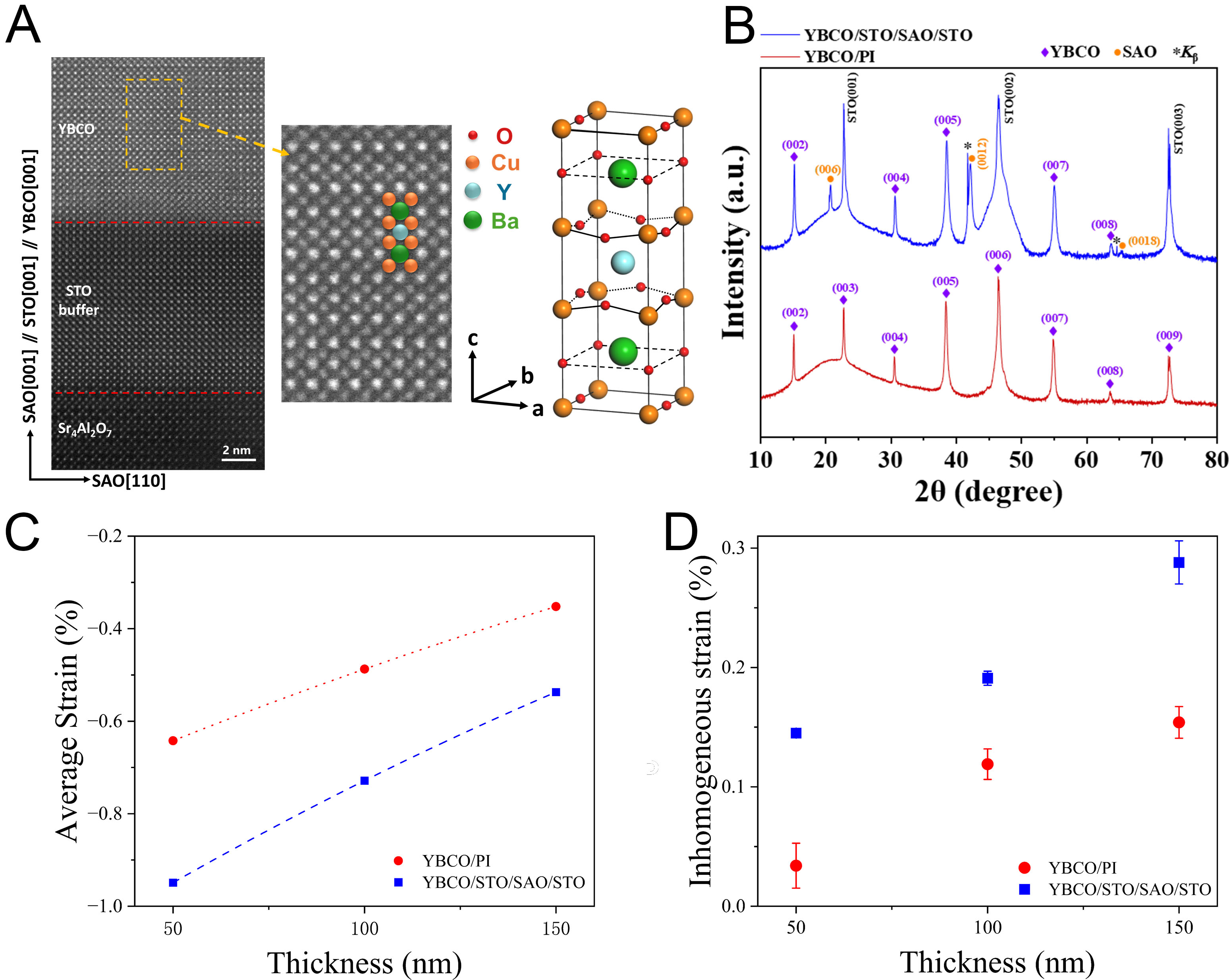
Figure 2. (A) Cross-sectional HAADF-STEM images of YBCO/STO/SAO structure. On the right is an enlarged view of the orange rectangle-enclosed region and a schematic diagram of the YBCO crystal structure; (B) XRD comparison of YBCO thin film before and after peeling and its corresponding structural diagram. Before peeling (blue), the YBCO (003), (006), and (009) diffraction peaks overlap with the STO (001), (002), and (003) peaks. After peeling (red), the YBCO (002) to (009) diffraction peaks are clearly visible; (C) Average out-of-plane strain as a function of thickness; (D) Inhomogeneous strain as a function of film thickness for different structures. The error bars originate from the standard error of the slope. YBCO: YBa2Cu3O7; STO: SrTiO3; SAO: Sr4Al2O7; HAADF-STEM: high-angle annular dark-field scanning transmission electron microscopy; XRD: X-ray diffraction.
Furthermore, quantitative analysis of the single-crystal diffraction peaks enables the determination of the c-axis lattice parameter in the different YBCO heterostructures. This allows the calculation of the average out-of-plane strain for YBCO thin films of various thicknesses through the relation:
where
To further investigate the effect of the strain induced by the peeling process, we performed Williamson-Hall (WH) analysis on the XRD θ-2θ scan results of YBCO films to study thickness-dependent strain gradients and their relaxation behavior[36] (As shown in Supplementary Figure 3). Figure 2D shows the variation of inhomogeneous strain with thickness before and after peeling. It can be observed that the inhomogeneous strain increases with film thickness, reflecting a broader local strain distribution during thickness-dependent relaxation, which remains incomplete even at 150 nm. These observations align with established strain relaxation mechanisms in complex oxides[13,37-39], YBCO thin films can release relaxation strain as the film thickness increases. Further investigations indicate that lattice mismatch is related to strain distribution. Recent studies suggest that strain is described as an internal distribution dependent on thickness t and the distance d from the film to the substrate interface[37,40,41]. Moreover, strain can also be released through other mechanisms. As shown in Figure 2D, the lift-off YBCO freestanding films exhibit markedly reduced inhomogeneous strain (εi) compared to their substrate-bound structures. Crucially, the observed inhomogeneous strain reduction directly correlates with a decrease in strain gradients, demonstrating that the peeling process not only enables fabrication of high-quality freestanding films but also partially relieves lattice-mismatch-induced strain gradients, which is beneficial for manufacturing high-quality flexible films with low strain gradients. It is worth noting that the persistence of inhomogeneous strain in the peeling films demonstrates that structural integrity preservation inherently precludes complete strain release. This limitation arises because the crack-free YBCO freestanding films maintain their macroscopic dimensions and crystalline continuity post-peeling; stress cannot be eliminated through microcrack formation. This preserved structural integrity enables further investigation of stress evolution and changes in physical properties. To further confirm that the observed Tc enhancement arises from strain modulation rather than changes in oxygen stoichiometry during the lift-off process, we performed micro-Raman spectroscopy before and after transfer [Supplementary Figure 4]. The O(4) apical oxygen mode analysis confirms that the YBCO film remains near the optimally oxygenated phase after lift-off, ruling out oxygen variation as a contributing factor.
To directly validate the in-plane strain behavior of the YBCO films before and after transfer, we performed asymmetric reciprocal space mapping (RSM) measurements on both the YBCO/STO/SAO/STO heterostructure and the transferred YBCO/PI film. For the YBCO/STO/SAO/STO heterostructure, clear and well-defined diffraction spots corresponding to YBCO (1 0 8), (1 0 9), and (1 0 10) asymmetric reflections are observed alongside the STO (103) substrate peak [Figure 3A], confirming the excellent epitaxial quality and high crystallinity of the as-grown YBCO film. Notably, the YBCO (1 0 9) peak nearly overlaps with the STO (103) peak, indicative of a strongly strained state imposed by substrate clamping. The transferred YBCO/PI films exhibit similar diffraction features, with corresponding asymmetric reflections clearly resolved [Figure 3B], confirming that the YBCO films retain their high crystalline quality after the lift-off process. A comparative analysis of the two RSM patterns reveals two distinct changes upon substrate removal. Along the out-of-plane Qz direction, the diffraction spots of the transferred YBCO film exhibit a pronounced narrowing in their vertical breadth. Since the vertical spread in reciprocal space directly correlates with the variation in c-axis lattice parameters, this narrowing provides unambiguous evidence that the out-of-plane strain gradient - inherently distributed along the film thickness due to interfacial clamping - is substantially minimized upon substrate removal, consistent with the symmetric XRD analysis presented above. On the other hand, along the in-plane Qx direction, a rightward expansion in the diffraction spots is observed, directly demonstrating a contraction of the in-plane lattice parameter toward its bulk optimal value. This provides clear experimental evidence for the relaxation of in-plane tensile strain following substrate removal. Consequently, the RSM results fundamentally substantiate that substrate removal successfully triggers in-plane tensile strain relaxation while simultaneously homogenizing the depth-dependent strain gradient throughout the film thickness, thereby synergistically driving the observed Tc enhancement and transition narrowing discussed in subsequent sections.
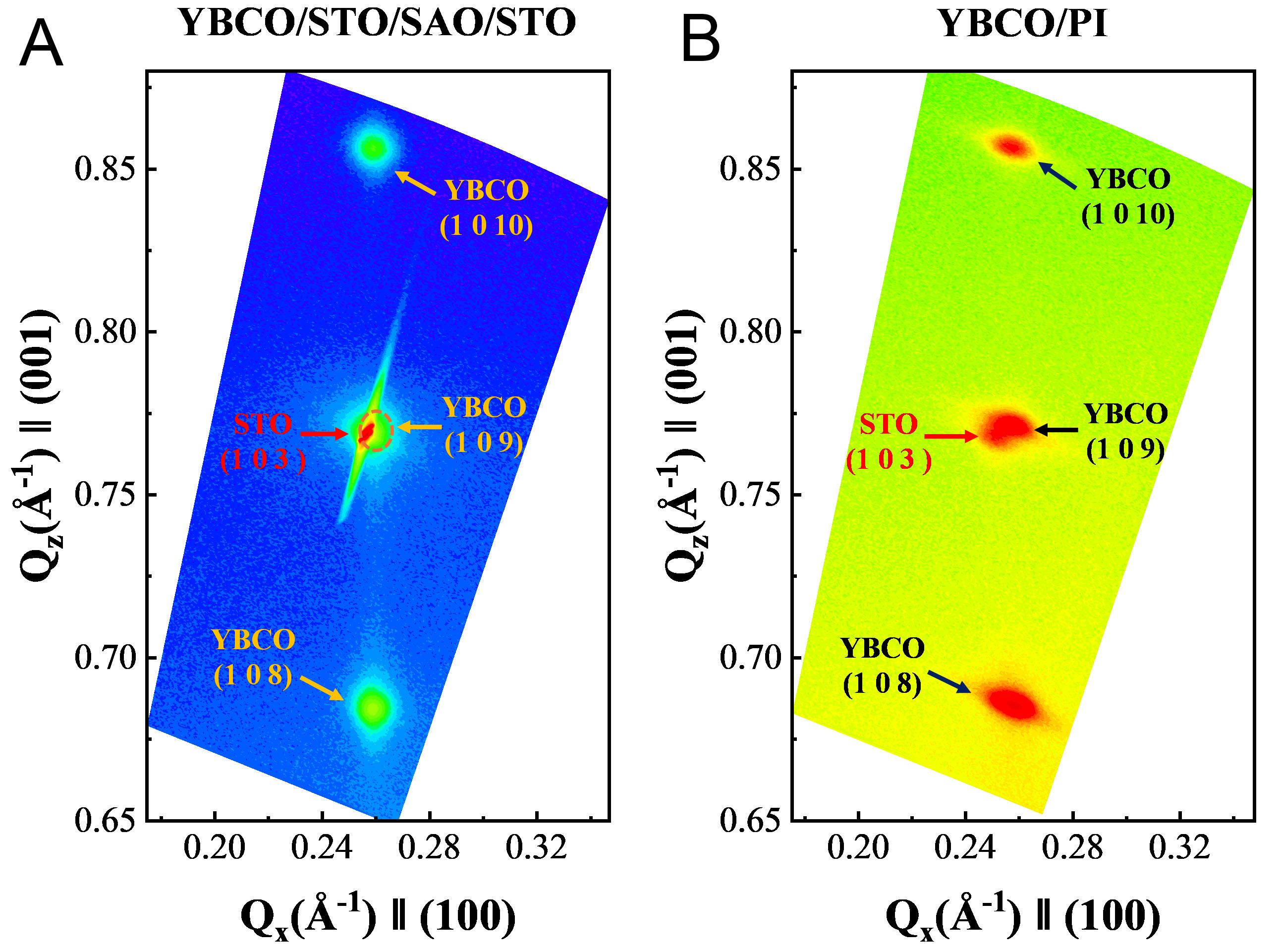
Figure 3. Reciprocal space mapping (RSM) analysis of strain states in YBCO films. (A) YBCO/STO/SAO/STO heterostructure, showing the close overlap between the YBCO (1 0 9) and STO (103) peaks, confirming coherent epitaxial growth under strong substrate clamping; (B) Transferred flexible YBCO/PI film. The YBCO (1 0 8), (1 0 9), and (1 0 10) reflections exhibit a sharpened profile along the Qz axis (decreased strain gradient) and a distinct rightward broadening along the Qx axis (in-plane strain relaxation toward bulk lattice parameters). YBCO: YBa2Cu3O7; STO: SrTiO3; SAO: Sr4Al2O7; PI: polyimide.
Superconductivity in flexible YBCO films
To investigate strain effects on the superconducting properties of YBCO, we performed temperature-dependent resistivity measurements using a standard four-point probe measurement (Physical Properties Measurement System, Quantum Design PPMS DynaCool, USA). The YBCO film thickness is 50 nm, with a 10-nm SrTiO3 buffer layer. At this thickness, the superconducting properties of the YBCO film are already close to their optimal values, as also confirmed by the transport results presented below. Furthermore, the STO buffer layer mentioned earlier serves both as a protective layer and as an epitaxial growth template that promotes c-axis-oriented growth of YBCO. Regarding potential interface effects, STO remains in a fully insulating dielectric state at temperatures around 90 K and does not compete with or couple to the superconducting transition of YBCO[42-44]. Therefore, the buffer layer does not affect the intrinsic superconductivity of the YBCO film. To ensure ohmic contact during measurement, 30-nm-thick Pt electrodes were deposited using magnetron sputtering (CHI-VAC Research & Development Co., Ltd.-CUSTOMIZED, China). Subsequently, photolithography (Durham Magneto Optics Microwriter ML II, UK) was used to etch electrode patterns on the sample surface for accurate resistivity measurements. Figure 4A presents comparative resistivity versus temperature (ρ-T) measurements for both the YBCO/STO/SAO/STO heterostructure and the peeling freestanding YBCO/PI film. The left inset shows an optical image of the electrode patterns, where the electrode central nanowire has dimensions of 100 μm in length and 20 μm in width. To ensure the accuracy of the experiment, the electrode will be maintained within the central region of the sample throughout the experiment. Both structures exhibit nearly identical temperature dependence, displaying characteristic metallic behavior (linear ρ-T relationship) above the critical temperature Tc. As the temperature approaches Tc, the resistivity drops sharply and approaches zero within a narrow transition width ΔT ≈ 1 K (defined as the temperature range from the critical temperature to the temperature where the resistivity is nearly zero, T95%ρ - T5%ρ). This indicates that the YBCO film has high crystal quality both before and after peeling.
The superconducting transition temperature Tc is defined as the critical temperature at the point of transition. The superconducting transition Tc of the structure before peeling was 90.1K at zero magnetic field, but the transition temperature Tc of the freestanding YBCO film was 91.2K. Consistently, as shown in Figure 4B, the freestanding YBCO/PI film demonstrates higher transition and zero-resistance temperatures than the YBCO/STO/SAO/STO structure under the same magnetic field (the raw data and detailed information under different magnetic fields are shown in Supplementary Figure 5). This systematic Tc elevation phenomenon suggests a strain-mediated improvement of superconducting properties, which may be mainly due to the change in in-plane tensile stress within the a-b planes. Furthermore, transport critical current density (Jc) measurements at 77 K confirm that the transfer process is non-destructive. Both the YBCO/STO/SAO/STO heterostructure and the flexible YBCO/PI film exhibit nearly identical Jc, demonstrating that no macroscopic structural damage occurs during the lift-off process [Supplementary Figure 6]. The YBCO lattice parameters (a = 3.82 Å, b = 3.89 Å)[34,45] are slightly smaller than the STO lattice constant (a = 3.905 Å). The SAO layer exhibits higher lattice flexibility and adjusts its lattice parameters according to other epitaxial layers[33]. Additionally, the thermal expansion coefficient of STO (α = 9.4 × 10⁻⁶/°C) is larger than that of YBCO (α = 8.6 × 10⁻⁶/°C), resulting in residual strain in the film after cooling to room temperature. Therefore, the YBCO film is in an in-plane tensile state within the YBCO/STO/SAO/STO structure. And there is no external stress perpendicular to the plane; the out-of-plane strain and in-plane strain components follow Poisson’s ratio:
To further investigate the effect of exfoliation on the superconducting properties of YBCO thin films at the macroscale, we independently designed and implemented a system based on the transmissive-type two-coil mutual inductance (TCMI) principle to measure the magnetic shielding response of samples before and after exfoliation (as illustrated schematically in Supplementary Figure 7A). The TCMI method operates based on the mutual inductance phenomenon between the drive coil and the receiving coil. When an alternating current (AC) with frequency f and amplitude Im is applied to the drive coil, the resulting time-varying magnetic flux through the receiving coil induces a corresponding voltage. Under constant excitation conditions, a smaller induced voltage reflects a weaker magnetic coupling between the coils. To enhance measurement flexibility and sensitivity, the coils were integrated onto a printed circuit board (PCB), as shown in the enlarged view of Supplementary Figure 7A and B. This design ensures a compact dimension while maintaining high adaptability for use in various cryogenic systems. The compact geometry, combined with a high turn density, effectively reduced magnetic flux leakage and enhanced signal intensity, thereby improving measurement precision and accuracy[50,51]. An excitation current Im = 0.3 mA was applied to the drive coil, while the in-phase component Vx and quadrature component Vy of the mutual inductance signal induced in the receiver coil were measured using a phase-locked amplifier. The temperature and time evolution of the real component (Vx) and imaginary component (Vy) of the mutual inductance signal for the sample before and after exfoliation are presented in Supplementary Figure 7C and D. In the transmissive TCMI device, when the sample is in the normal state, the magnetic field generated by the drive coil can directly penetrate the sample and reach the pickup coil. In this case, the induced voltage corresponds to the bare mutual inductance between the two coils, which is solely determined by their geometric parameters and separation distance. As the temperature decreases, the film first enters the vortex state (also known as the mixed state). In this state, quantized magnetic flux lines penetrate the film, each forming a normal-state core surrounded by supercurrents, as illustrated in Figure 4C. Structural inhomogeneities in the film may result in differing transition temperatures across regions or modify the effective density of pinning centers. This macroscopically broadens the temperature range of the vortex state, corresponding to slower magnetic shielding, and is typically difficult to observe in localized measurements. Upon the film transition to the superconducting state, it expels the magnetic field, exhibiting a magnetic shielding response. This Meissner effect of the superconductor markedly weakens the magnetic coupling between the coils, leading to a marked reduction in the magnetic flux at the receiving coil and a consequent sharp decrease in the induced voltage (as schematically illustrated in the inset of Figure 4D). Furthermore, analogous to AC magnetic susceptibility measurements[52], energy dissipation gives rise to an imaginary component of the induced voltage. This dissipative response manifests as a characteristic peak near the superconducting transition temperature, reflecting vortex dynamics and associated loss mechanisms.
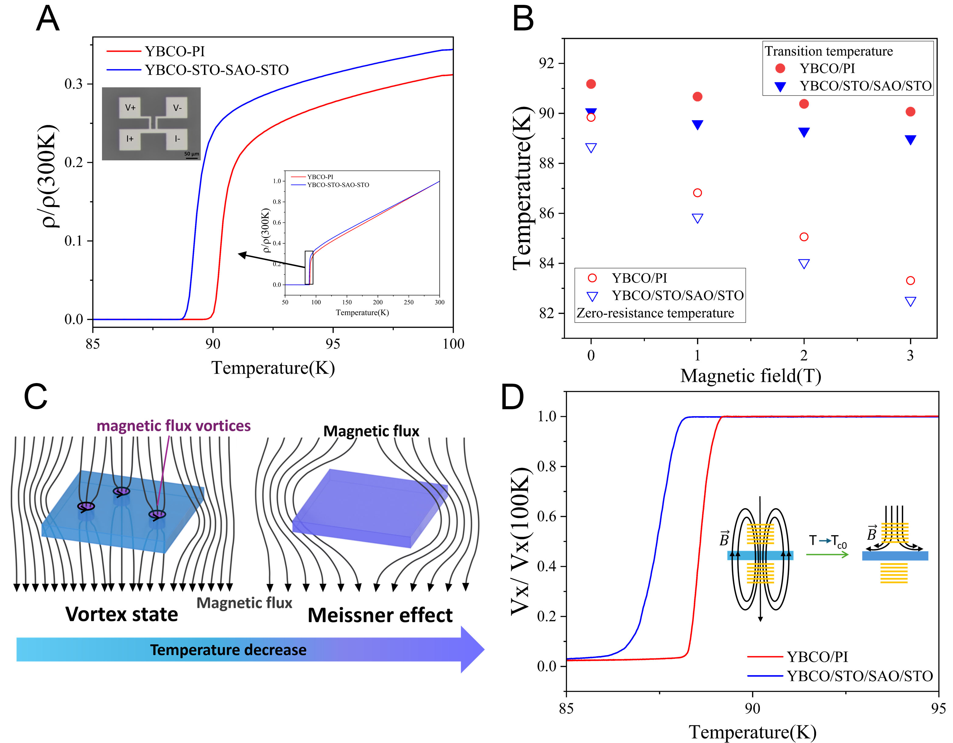
Figure 4. Comparison of electrical tests before and after YBCO peeling. (A) Resistivity-temperature (85K-100K) test curves of YBCO thin films before (blue) and after (red) peeling, with an inset on the right showing the complete image of the 50K-300K test. The image on the left shows the photolithographic structure for four-probe resistance testing; (B) Transition temperature and zero-resistance temperature before and after peeling under different magnetic fields; (C) Schematic diagram of magnetic response across the superconducting transition; (D) Comparison of induced voltage Vx(T) before and after peeling, with an inset showing a schematic diagram of the coil measurement of superconducting samples. YBCO: YBa2Cu3O7; PI: polyimide; STO: SrTiO3; SAO: Sr4Al2O7. Vx: real component.
In TCMI measurements of superconducting samples, the real and imaginary components of the induced voltage reflect different physical mechanisms. The real component Vx reflects the superconductor’s magnetic shielding capability against the magnetic field. The temperature at which Vx exhibits an abrupt transition corresponds to the onset temperature of the Meissner effect, while its low-temperature value reflects the strength of the sample’s superconducting magnetic shielding. The imaginary component Vy arises from energy dissipation in the superconductor under the alternating magnetic field, primarily due to magnetic flux motion or thermal fluctuations[53,54]. Its peak signifies the large-scale vortex motion, and its full width at half maximum can reflect the sample’s quality - narrower FWHM values correspond to a more uniform sample. In comparison, as shown in Figure 4D, first, the onset of magnetic shielding response (
The results of the TCMI test also indicate that the delamination process may have affected the intrinsic superconducting mechanism of YBCO. On the one hand, according to the London equation,
Strain-modulated superconductivity in YBCO flexible films
The stress-mediated modulation of flexible electronic materials and their associated property changes remain a focal point of research interest, as they are crucial for understanding underlying physical mechanisms and enabling future practical applications[56-58]. However, due to technical limitations, continuous strain regulation in flexible high-temperature superconducting films still faces critical research gaps that need to be addressed. Based on our freestanding film fabrication technique, we conducted further continuous bending tests on high‑quality flexible YBCO films, and the experimental results are presented in Figure 5. Previously, direct optical microscopy of the film surface was performed before and after a complete bending cycle. No cracks or structural damage formed after bending, confirming that the flexible YBCO film exhibits excellent bending stability [Supplementary Figure 8]. To perform bending tests, we fabricated curved molds with different curvatures (κ). The flexible YBCO film is supported on a PI substrate with a thickness t = 0.1 mm and exhibits exceptional flexibility and bendability. Due to the compliant nature of the sample structure, it can be readily attached to the surface of each mold with minimal mechanical force, without requiring adhesives or additional processing steps, and remain crack-free throughout the procedure. This facilitates convenient and rapid switching between molds for continuous testing under different bending conditions. To ensure stable electrical contact during mold exchange and repeated handling, the electrode regions were locally reinforced with silver paste. When the sample was completely and conformally attached to the mold, the mold induced strain through stresses derived from the bent epitaxial film.
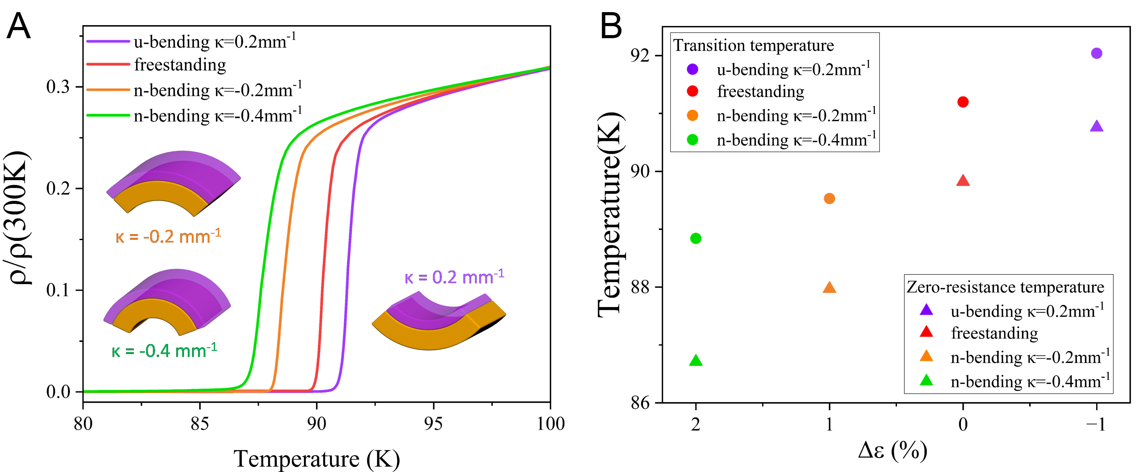
Figure 5. (A) Resistivity versus temperature (80 K-100 K) of a flexible YBCO thin film under different bending states, with insets illustrating the corresponding bending configurations at varying curvatures; (B) Transition temperature and zeroresistance temperature extracted from each bending condition. YBCO: YBa2Cu3O7.
In a standalone PI layer, the neutral axis coincides with the geometric center of the PI, resulting in a linear variation of bending strain along the direction of thickness. For the composite structure consisting of a thin film bonded to a PI substrate, the difference in Young’s modulus between the film and the substrate leads to a shift in the neutral axis by Δδ to satisfy overall force balance. Consequently, the local strain in the film can be expressed as
To assess the effect of strain on superconducting properties, we measure the flexible YBCO film under unbent conditions as a control group (red curve in Figure 5A), which exhibited excellent superconducting properties. To verify the film’s bendability during testing, tensile strain experiments - which are more susceptible to inducing cracks - were first performed using a mold with curvature κ = -0.2 mm-1 (orange curve in Figure 5A). Under this tensile strain, the superconducting transition temperature decreases to approximately 89.5 K, indicating that tensile strain suppresses the superconductivity of the flexible YBCO film. As the tensile strain increases further, superconducting performance decreases accordingly, confirming that larger in-plane tensile strain is detrimental to YBCO’s superconducting transition. This observation is similar to the trend of Tc variation induced by strain changes during the transfer process. Subsequent measurements under in-plane compressive strain (purple curve in Figure 5A) reveal an enhanced superconducting transition temperature (Tc), approaching the value observed in bulk YBCO. This result indicates that an appropriate in-plane compressive strain can effectively enhance the superconductivity of flexible YBCO thin films. To further verify reproducibility, we additionally conducted three consecutive mounting-demounting cycles under each bending condition; the resulting show excellent repeatability with standard deviations substantially smaller than the bending-induced Tc shift [Supplementary Figure 9], confirming the statistical significance of the strain-dependent modulation. The reproducibility of the results and the reversible nature of the strain-dependent behavior suggest that no microcracks were formed during the bending tests, further demonstrating the outstanding flexibility of the sample. Figure 5B presents the superconducting Tc and the zero-resistance temperature (T0) corresponding to the applied in-plane bending strain Δε; these results provide a direct illustration of how continuous mechanical strain influences the superconductivity of flexible YBCO thin films. Notably, under larger tensile strains (Δε = 2%), a broadening of the superconducting transition is observed, potentially due to the inhomogeneity of the superconducting region caused by excessive strain. This strain-mediated continuous modulation of superconducting properties also accounts for the previously observed phenomenon of enhanced Tc following flexible film transfer.
While the precise physical mechanisms require further elucidation, these findings are still very interesting and reveal a noteworthy phenomenon: in-plane strain can effectively modulate the superconducting properties of YBCO films. The transfer results indicate that the YBCO film in the YBCO/STO/SAO/STO heterostructure experiences in-plane tensile stress, which is partially relieved during peeling, corresponding to changes in the lattice structure. The improvements in both Tc and magnetic shielding response can be attributed to the reduction of a-b plane tensile strain and its gradient after lift-off. This strain release drives the system closer to the intrinsic superconducting characteristics of stress-free YBCO bulk material. Furthermore, strain mediation not only enables continuous tuning of the superconductivity in YBCO but also elevates the superconducting transition temperature of the flexible film to a level previously unattainable. These findings address a gap in previous research. In the field of flexible electronics, the superconducting properties and structural integrity of the freestanding YBCO films produced by this method also surpass those of previously demonstrated systems. Furthermore, this stress-release mechanism during the peeling process may offer broader implications and has certain reference value for other research fields and systems. Future studies employing in situ strain measurements combined with advanced microstructural characterization could provide deeper insights into these phenomena. In particular, systematic investigations correlating real-time strain evolution with superconducting mechanisms may elucidate the complex interplay between lattice defects, flux pinning, and electronic properties.
CONCLUSIONS
In conclusion, we have successfully prepared high-quality, large-size, crack-free YBCO freestanding thin films by selectively etching the water-soluble sacrificial layer Sr4Al2O7. Experimental studies reveal that the aqueous peeling process can effectively release part of the strain and strain gradients induced by lattice mismatch during heteroepitaxial growth, driving the freestanding thin film closer to a stress-free state. Further electrical transport and magnetic shielding response demonstrate that freestanding YBCO thin films exhibit pronounced enhancements in both superconducting transition temperature and Meissner shielding capability. Subsequent continuous strain-modulation experiments successfully regulated the superconducting properties of flexible YBCO thin films, with enhanced superconductivity obtained under compressive strain. These results confirm the high crystallinity and strong superconducting properties achieved in the freestanding YBCO film. This achievement contributes to a deeper understanding of the physical relationship between the structure of YBCO and its intrinsic properties. It also facilitates the integration and application of high-temperature superconductors in flexible electronic systems.
DECLARATIONS
Authors’ contributions
Led the entire project and wrote the main manuscript text: Wang, Z.
Participated throughout the project: Liu, B.
Was responsible for the film growth work: Liu, B.; Shen, D.
Performed the TEM analysis: Zhou, X.; Zhang, B.
Provided support for electrical transport studies and measurements: Li, D.; Sun, Y.
Assisted with the growth and transfer of the water-soluble layer SAO films: Li, M.
Did the simulation work and provided guidance: Wong, C. H.
Were responsible for the whole project and paper proofreading: Zhang, J.; Dai, J. Y.
Availability of data and materials
The data supporting the findings of this study are available within this Article and its Supplementary Materials. Further data are available from the corresponding authors upon reasonable request.
AI and AI-assisted tools statement
Not applicable.
Financial support and sponsorship
This work was supported by the Guangdong Provincial Quantum Science Strategic Initiative (Grant No. GDZX2501006), the National Natural Science Foundation of China (Grant No.52225205, No. 12550004, No. U23A20366 and No. 12304073) and the Beijing Natural Science Foundation (Grant No. Z240008).
Conflict of Interests
Li, D. is a Guest Editor of the special issue “Microstructure Engineering of Superconducting Thin Films and Interfaces” of the journal Microstructures. Li, D. was not involved in any steps of editorial processing, including reviewers’ selection, manuscript handling, and decision-making. The other authors declare no conflicts of interest.
Ethical approval and consent to participate
Not applicable.
Consent for publication
Not applicable.
Copyright
© The Author(s) 2026.
Supplementary Materials
REFERENCES
1. Keimer, B.; Kivelson, S. A.; Norman, M. R.; Uchida, S.; Zaanen, J. From quantum matter to high-temperature superconductivity in copper oxides. Nature 2015, 518, 179-86.
2. Novoselov, K. S.; Mishchenko, A.; Carvalho, A.; Castro, Neto. A. H. 2D materials and van der Waals heterostructures. Science 2016, 353, aac9439.
3. Neto AH, Guinea F, Peres NMR, Novoselov KS, Geim AK. The electronic properties of graphene. Rev. Mod. Phys. 2009, 81, 109-62.
4. Manzeli, S.; Ovchinnikov, D.; Pasquier, D.; Yazyev, O. V.; Kis, A. 2D transition metal dichalcogenides. Nat. Rev. Mater. 2017, 2, BFnatrevmats201733.
5. Okada, M.; Okigawa, Y.; Kubo, T.; Nakajima, H.; Yamada, T. Strain engineering of MoS2 by tuning the transfer process. ACS. Appl. Electron. Mater. 2025, 7, 3590-8.
6. Hwang, H. Y.; Iwasa, Y.; Kawasaki, M.; Keimer, B.; Nagaosa, N.; Tokura, Y. Emergent phenomena at oxide interfaces. Nat. Mater. 2012, 11, 103-13.
7. Stemmer, S.; James, Allen. S. Two-dimensional electron gases at complex oxide interfaces. Annu. Rev. Mater. Res. 2014, 44, 151-71.
8. Chakhalian, J.; Freeland, J. W.; Millis, A. J.; Panagopoulos, C.; Rondinelli, J. M. Colloquium: emergent properties in plane view: strong correlations at oxide interfaces. Rev. Mod. Phys. 2014, 86, 1189-202.
9. Bhattacharya, A.; May, S. J. Magnetic oxide heterostructures. Annu. Rev. Mater. Res. 2014, 44, 65-90.
10. Ramesh, R.; Schlom, D. G. Creating emergent phenomena in oxide superlattices. Nat. Rev. Mater. 2019, 4, 257-68.
12. Zhang, F.; Lv, P.; Zhang, Y.; et al. Modulating the electrical transport in the two-dimensional electron gas at LaAlO3/SrTiO3 heterostructures by interfacial flexoelectricity. Phys. Rev. Lett. 2019, 122, 257601.
13. Liu, X.; Hu, T.; Zhang, Y.; et al. Flexomagnetoelectric effect in Sr2IrO4 thin films. Phys. Rev. Lett. 2024, 133, 156505.
14. Spaldin, N. A.; Ramesh, R. Advances in magnetoelectric multiferroics. Nat. Mater. 2019, 18, 203-12.
15. Wadehra, N.; Gregory, B. Z.; Zhang, S.; et al. Strain-induced superconductivity in RuO2(100) thin-films. Commun. Mater. 2025, 6, 856.
16. Zhao, S. Y. F.; Cui, X.; Volkov, P. A.; et al. Time-reversal symmetry breaking superconductivity between twisted cuprate superconductors. Science 2023, 382, 1422-7.
17. Cao, Y.; Fatemi, V.; Fang, S.; et al. Unconventional superconductivity in magic-angle graphene superlattices. Nature 2018, 556, 43-50.
18. Cao, Y.; Fatemi, V.; Demir, A.; et al. Correlated insulator behaviour at half-filling in magic-angle graphene superlattices. Nature 2018, 556, 80-4.
19. Tarnopolsky, G.; Kruchkov, A. J.; Vishwanath, A. Origin of magic angles in twisted bilayer graphene. Phys. Rev. Lett. 2019, 122, 106405.
20. Wu, X. D.; Foltyn, S. R.; Arendt, P.; et al. High current YBa2Cu3O7-δ thick films on flexible nickel substrates with textured buffer layers. Appl. Phys. Lett. 1994, 65, 1961-3.
21. Pan, A. V.; Pysarenko, S.; Dou, S. X. Drastic improvement of surface structure and current-carrying ability in YBa2Cu3O7 films by introducing multilayered structure. Appl. Phys. Lett. 2006, 88, 232506.
22. Pan, A.; Pysarenko, S.; Wexler, D.; Rubanov, S.; Dou, S. Multilayering and Ag-doping for properties and performance enhancement in YBa2Cu3O7 films. IEEE. Trans. Appl. Supercond. 2007, 17, 3585-8.
23. Paull, O. H. C.; Pan, A. V.; Causer, G. L.; et al. Field dependence of the ferromagnetic/superconducting proximity effect in a YBCO/STO/LCMO multilayer. Nanoscale 2018, 10, 18995-9003.
24. Ran, Q.; Jing, Z.; Shen, L.; et al. Suppression of flux avalanches in YBCO superconducting thin films by coating metal investigated using magneto-optical imaging. Superconductivity 2024, 11, 100101.
25. Li, L.; Lei, L.; Zhao, G.; Deng, B.; Yan, F.; Li, C. Highly epitaxial YBa2Cu3O7-δ films grown on gradient La2-xGdxZr2O7 -buffered NiW-RABiTS using all sol-gel process. Supercond. Sci. Technol. 2021, 34, 045004.
26. Chen, Z.; Wang, B. Y.; Goodge, B. H.; et al. Freestanding crystalline YBa2Cu3O7-x heterostructure membranes. Phys. Rev. Materials. 2019, 3, 060801.
27. Chiabrera, F. M.; Yun, S.; Li, Y.; et al. Freestanding perovskite oxide films: synthesis, challenges, and properties. Annalen. der. Physik. 2022, 534, 2200084.
28. Pesquera, D.; Fernández, A.; Khestanova, E.; Martin, L. W. Freestanding complex-oxide membranes. J. Phys. Condens. Matter. 2022, 34.
29. Jia, Z.; Tang, C. S.; Wu, J.; et al. Self-passivated freestanding superconducting oxide film for flexible electronics. Appl. Phys. Rev. 2023, 10, 031401.
30. Favre, S.; Ariosa, D.; Yelpo, C.; Mazini, M.; Faccio, R. Depression of critical temperature due to residual strain induced by PLD deposition on YBa2Cu3O7-δ thin films. Mater. Chem. Phys. 2021, 266, 124507.
31. Liu, B.; Liu, Z.; Li, M.; Zhang, Y.; Wang, A. Large-size damage-free transfer of perovskite oxide films by controllable thermal gradient. Nano. Res. 2026, 19, 94908225.
32. Lu, D.; Baek, D. J.; Hong, S. S.; Kourkoutis, L. F.; Hikita, Y.; Hwang, H. Y. Synthesis of freestanding single-crystal perovskite films and heterostructures by etching of sacrificial water-soluble layers. Nat. Mater. 2016, 15, 1255-60.
33. Zhang, J.; Lin, T.; Wang, A.; et al. Super-tetragonal Sr4Al2O7 as a sacrificial layer for high-integrity freestanding oxide membranes. Science 2024, 383, 388-94.
34. Liang, R.; Dosanjh, P.; Bonn, D.; Baar, D.; Carolan, J.; Hardy, W. Growth and properties of superconducting YBCO single crystals. Physica. C. 1992, 195, 51-8.
35. Liang, R.; Bonn, D.; Hardy, W. Growth of high quality YBCO single crystals using BaZrO3 crucibles. Physica. C. 1998, 304, 105-11.
36. Williamson, G.; Hall, W. X-ray line broadening from filed aluminium and wolfram. Acta. Metallurgica. 1953, 1, 22-31.
37. Catalan, G.; Noheda, B.; Mcaneney, J.; Sinnamon, L. J.; Gregg, J. M. Strain gradients in epitaxial ferroelectrics. Phys. Rev. B. 2005, 72.
38. Sando, D.; Appert, F.; Burns, S. R.; et al. Influence of flexoelectricity on the spin cycloid in (110)-oriented BiFeO3 films. Phys. Rev. Materials. 2019, 3.
39. Jeon, B. C.; Lee, D.; Lee, M. H.; et al. Flexoelectric effect in the reversal of self-polarization and associated changes in the electronic functional properties of BiFeO3 thin films. Adv. Mater. 2013, 25, 5643-9.
40. Chu, M. W.; Szafraniak, I.; Scholz, R.; et al. Impact of misfit dislocations on the polarization instability of epitaxial nanostructured ferroelectric perovskites. Nat. Mater. 2004, 3, 87-90.
41. Nicola, L.; Vandergiessen, E.; Gurtin, M. Effect of defect energy on strain-gradient predictions of confined single-crystal plasticity. J. Mech. Phys. Solids. 2005, 53, 1280-94.
42. Wahlberg, E.; Arpaia, R.; Chakraborty, D.; et al. Boosting superconductivity in ultrathin YBa2Cu3O7-δ films via nanofaceted substrates. Nat. Commun. 2026, 17, 285.
43. Mirarchi, G.; Arpaia, R.; Wahlberg, E.; et al. Tuning the ground state of cuprate superconducting thin films by nanofaceted substrates. Commun. Mater. 2024, 5, 582.
44. Liu, Y.; Meng, Q.; Mahmoudi, P.; et al. Advancing superconductivity with interface engineering. Adv. Mater. 2024, 36, e2405009.
45. Zhai, H. Y.; Chu, W. K. Effect of interfacial strain on critical temperature of YBa2Cu3O7-δ thin films. Appl. Phys. Lett. 2000, 76, 3469-71.
46. Dunn, M. L.; Ledbetter, H. Poisson’s ratio of porous and microcracked solids: Theory and application to oxide superconductors. J. Mater. Res. 1995, 10, 2715-22.
48. Welp, U.; Grimsditch, M.; Fleshler, S.; et al. Effect of uniaxial stress on the superconducting transition in YBa2Cu3O7. Phys. Rev. Lett. 1992, 69, 2130-3.
49. Meingast, C.; Kraut, O.; Wolf, T.; Wühl, H.; Erb, A.; Müller-Vogt, G. Large a-b anisotropy of the expansivity anomaly at Tc in untwinned YBa2Cu3O7- delta. Phys. Rev. Lett. 1991, 67, 1634-7.
50. Claassen, J. H.; Wilson, M. L.; Byers, J. M.; Adrian, S. Optimizing the two-coil mutual inductance measurement of the superconducting penetration depth in thin films. J. Appl. Phys. 1997, 82, 3028-34.
51. Turneaure, S. J.; Pesetski, A. A.; Lemberger, T. R. Numerical modeling and experimental considerations for a two-coil apparatus to measure the complex conductivity of superconducting films. J. Appl. Phys. 1998, 83, 4334-43.
52. Hein, R. A. ac magnetic susceptibility, Meissner effect, and bulk superconductivity. Phys. Rev. B. Condens. Matter. 1986, 33, 7539-49.
53. Zhang, R.; Zhao, Z.; Qin, M.; et al. Determining the thickness of the dead layer in superconducting film using a two-coil mutual-inductance technique. Phys. Rev. Applied. 2022, 17, 054034.
54. Liu, N.; Yao, G.; Qu, Y.; et al. Calculation of penetration depth under various numerical models for the reflection-type two-coil mutual inductance technique. Supercond. Sci. Technol. 2023, 36, 035006.
55. Zhang, R. Z.; Qin, M. Y.; Zhang, L.; et al. Measurement of magnetic penetration depth in superconducting films by two-coil mutual inductance technique. Acta. Phys. Sin. 2020, 69, 047401.
56. Nair, S.; Yang, Z.; Lee, D.; et al. Engineering metal oxidation using epitaxial strain. Nat. Nanotechnol. 2023, 18, 1005-11.
57. Geng, W.; Wang, Y.; Tang, Y.; et al. Atomic-scale tunable flexoelectric couplings in oxide multiferroics. Nano. Lett. 2021, 21, 9601-8.
Cite This Article
 Open Access
How to Cite
Wang, Z.; Liu, B.; Shen, D.; Zhou, X.; Li, D.; Sun, Y. J.; Li, M.; Zhang, B.; Wong, C. H.; Zhang, J.; Dai, J.Y. Strain-modulation and enhancement of superconductivity in flexible YBa2Cu3O7 thin films. Microstructures 2026, 6, 20260122. https://dx.doi.org/10.20517/microstructures.2026.92
Download Citation
Export Citation File:
Type of Import
Tips on Downloading Citation
Citation Manager File Format
Type of Import
Direct Import: When the Direct Import option is selected (the default state), a dialogue box will give you the option to Save or Open the downloaded citation data. Choosing Open will either launch your citation manager or give you a choice of applications with which to use the metadata. The Save option saves the file locally for later use.
Indirect Import: When the Indirect Import option is selected, the metadata is displayed and may be copied and pasted as needed.
About This Article
Special Topic
Copyright

Data & Comments
Data
0







Comments
Comments must be written in English. Spam, offensive content, impersonation, and private information will not be permitted. If any comment is reported and identified as inappropriate content by OAE staff, the comment will be removed without notice. If you have any queries or need any help, please contact us at support@oaepublish.com.