



fig4

Tailoring microstructure engineering to decouple electron-phonon transport in Se-based thermoelectric alloys

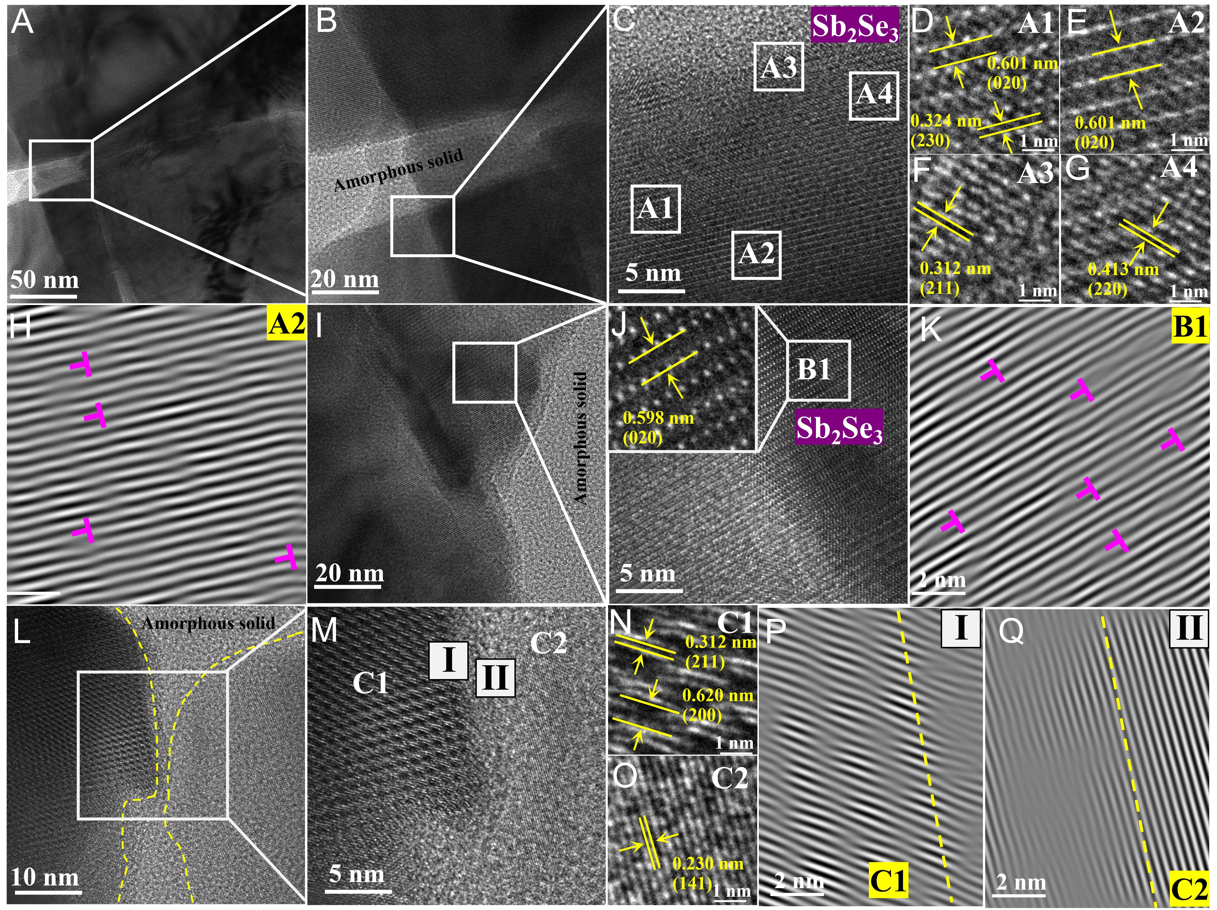
Figure 4. Microstructure characterization of the Sb-Se system. (A-C) TEM images at progressively higher magnifications: 50, 20, and 5 nm scales; (D-G) Lattice analysis diagrams corresponding to regions A1, A2, A3, and A4 in (C), respectively; (H) Atomic dislocation map of region A2; (I-M) Additional TEM images and magnified views: (I) at 20 nm, (J) further magnified, (L) at 10 nm, and (M) at 5 nm scales. (K) Atomic dislocation map of region B1; (N and O) Lattice analysis diagrams of regions C1 and C2, respectively; (P and Q) Atomic dislocation maps of region I and region II, respectively. TEM: Transmission electron microscopy.

Microstructures
ISSN 2770-2995 (Online)

Portico

All published articles are preserved here permanently:

https://www.portico.org/publishers/oae/

Portico

All published articles are preserved here permanently:

https://www.portico.org/publishers/oae/