



fig3
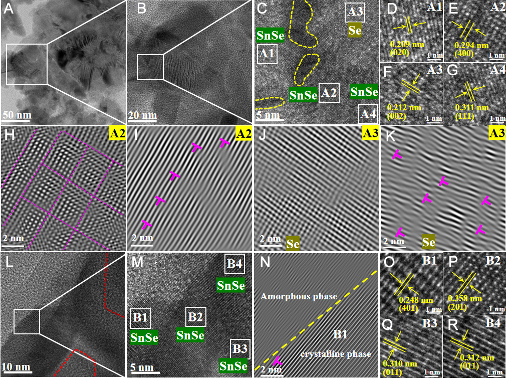
Figure 3. Microstructure characterization of the Sn-Se system. (A-C) TEM images at successively higher magnifications: 50, 20, and 5 nm scales; (D-G) Lattice analysis diagrams corresponding to regions A1, A2, A3, and A4 in (C), respectively; (H and I) Atomic arrangement and dislocation diagrams for region A2; (J and K) the corresponding diagrams for region A3; (L and M) TEM images at 10 nm and 5 nm scales, respectively; (N) Atomic dislocation diagram at the interface between the crystalline region B1 and the amorphous domain; (O-R) Lattice analysis diagrams for regions B1 to B4 in (M). TEM: Transmission electron microscopy.