



fig2
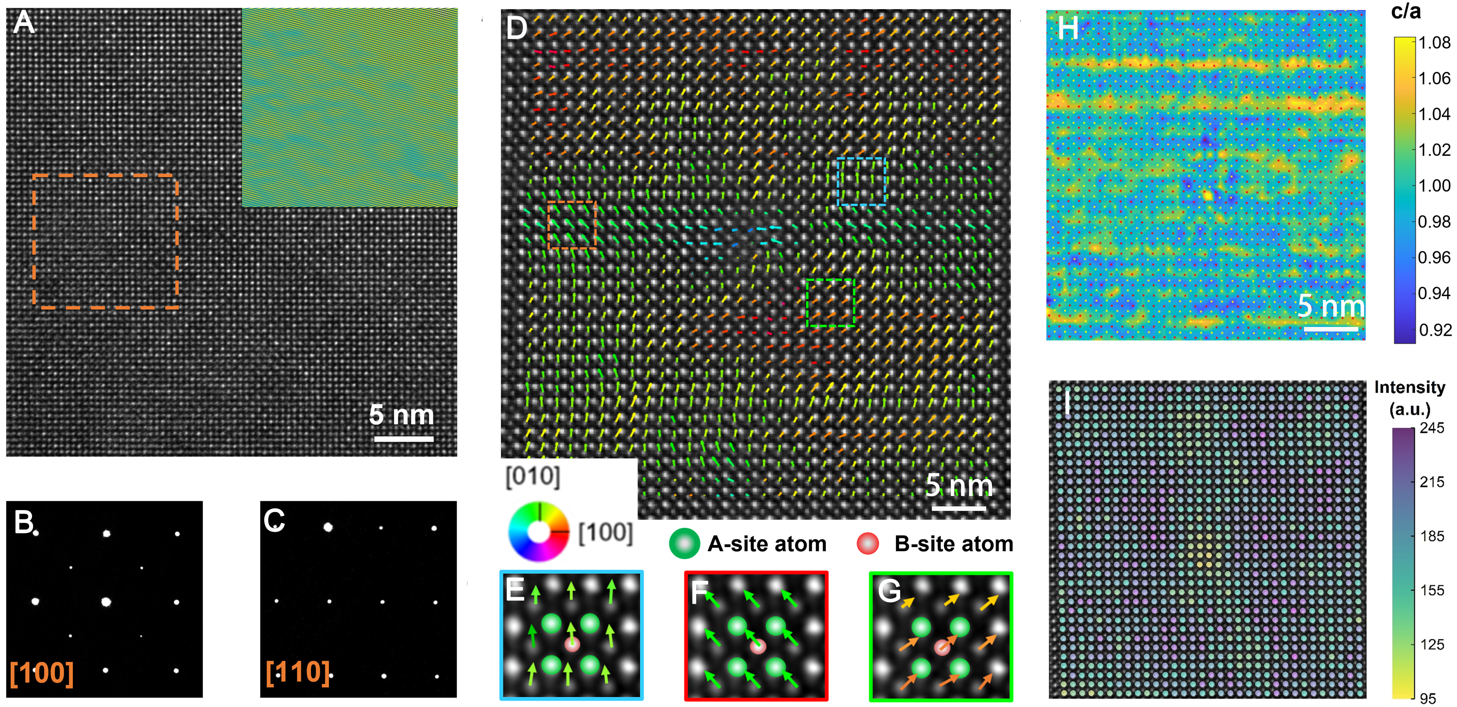
Figure 2. Microscopic structure of BNT-BT-0.1BS ceramic observed by electron microscopy. (A) High-resolution TEM image and corresponding IFFT pattern in the inset; (B and C) SAED patterns along the [001]c and [110]c directions; (D) HAADF-STEM image recorded along the [100]c direction and the corresponding atomic displacement vector mapping; (E-G) Enlarged B-site displacement vectors of the boxed region in (D). Corresponding (H) c/a ratio, and (I) atomic intensity mapping of (D). BNT: Bi0.5Na0.5TiO3; BT: BaTiO3; BS: BaSnO3; TEM: transmission electron microscope; IFFT: inverse fast Fourier transform; SAED: selected area electron diffraction; HAADF-STEM: high-angle annular dark-field scanning transmission electron microscopy.