fig7
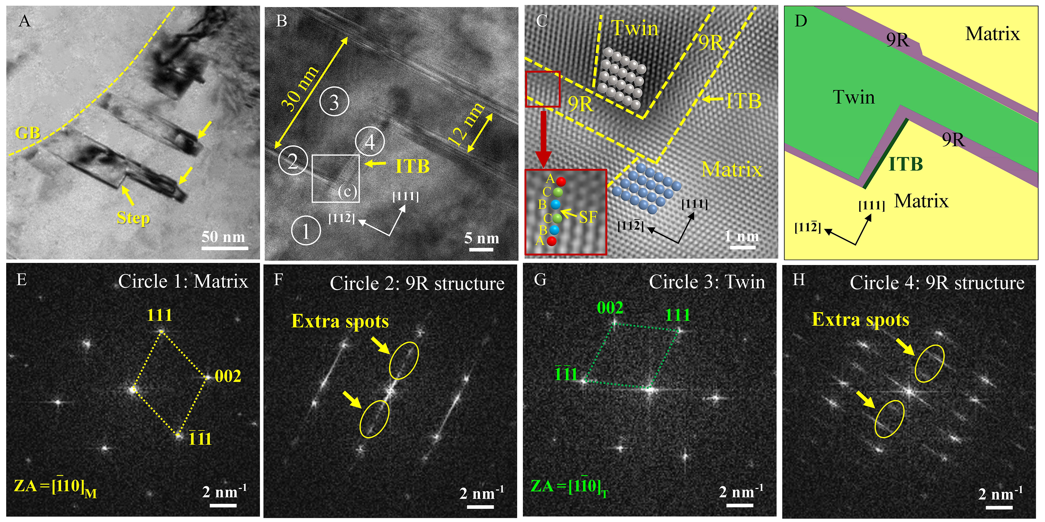
Figure 7. TEM results of twins with a stepped morphology partially extending through the grain: (A) BF image; (B) HRTEM image; (C) IFFT image of the region marked by the white square in (B); (D) structural distribution map of (B); (E-H) FFT images of the regions marked by white circles 1-4 in (B). BF: Bright field; HRTEM: high-resolution transmission electron microscopy; IFFT: inverse fast Fourier transform; FFT: fast Fourier transform; ITB: incoherent twin boundary; GB: grain boundary; SF: stacking fault; ZA: zone axis; M: matrix.