



fig5
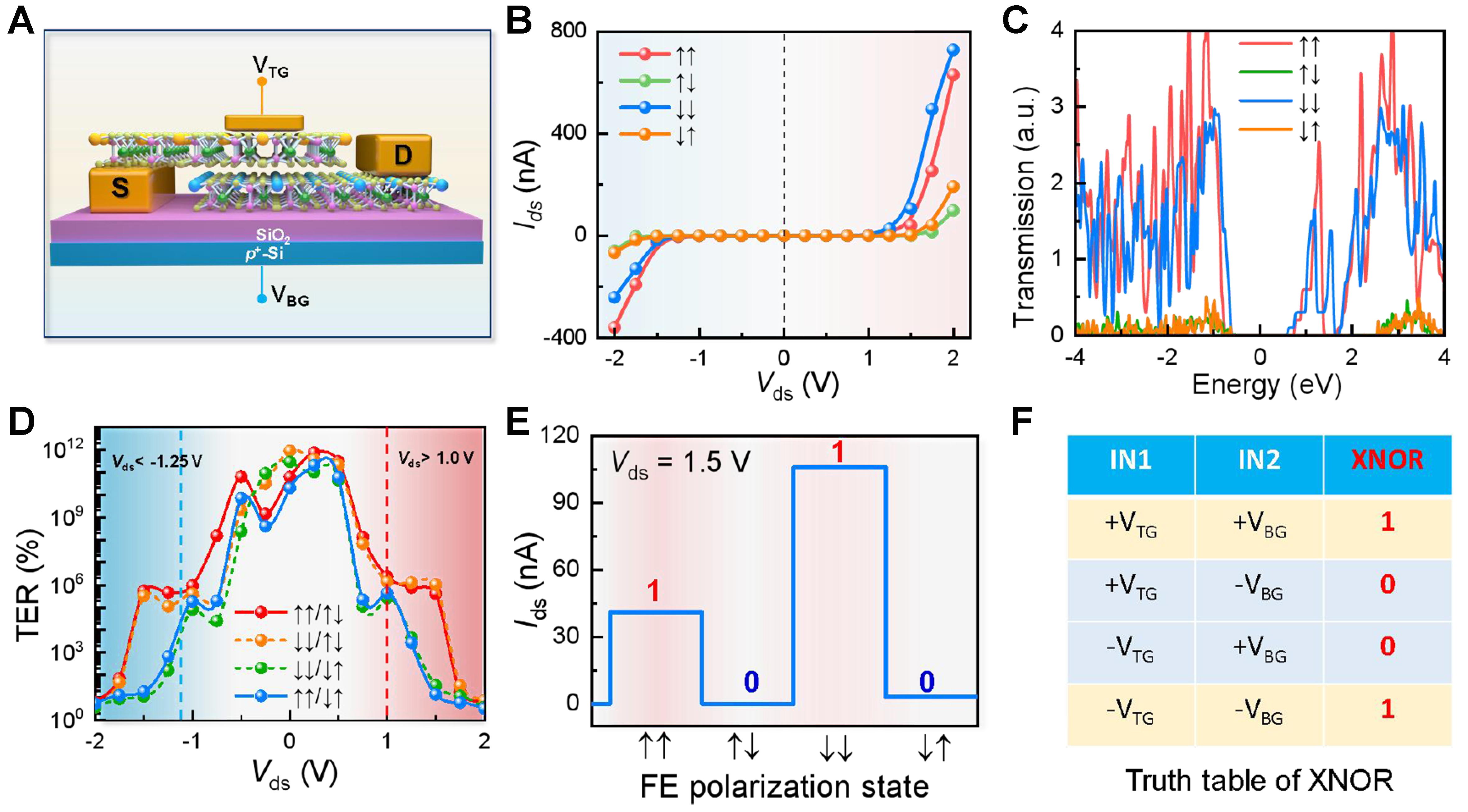
Figure 5. Effect of multiple polarization states on electrical transport of CIPS/AIPS VFSH device. (A) Schematic diagram of CIPS/AIPS transistor structure; (B) Ids-Vds curves of CIPS/AIPS device in four polarization states; (C) Transmission spectra of CIPS/AIPS device in four polarization states; (D) TER of CIPS/AIPS device as a function of Vds; (E) Ids of CIPS/AIPS device in four polarization states at Vds = 1.5 V. The Ids of four polarization states is larger than 10 nA as the logic output “1” and lower than 10 nA as the logic output “0”; (F) Truth table of XNOR logic operation. Here +VTG and +VBG represent logic input “1”, and -VTG and -VBG represent logic input “0”. CIPS/AIPS: CuInP2S6/AuInP2S6; VFSH: vdW FE semiconductor heterojunction; TER: tunneling electroresistance ratio.