



Computational screening of reconfigurable van der Waals ferroelectric semiconductor heterojunctions for all-in-one optoelectronic devices
 0
Abstract
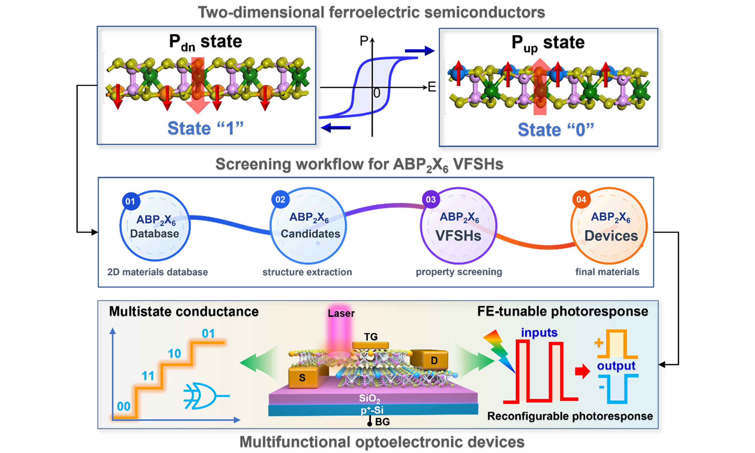
Reconfigurable optoelectronic devices based on two-dimensional (2D) van der Waals semiconductor heterojunctions (VSHs) are potential candidates for multifunctional applications in a single device. However, device multifunctionalities highly rely on VSHs with tunable band alignment and band offsets for achieving reconfigurable optoelectronic properties. Herein, we report a new class of 2D VSHs consisting of atomically thin ABP2X6-type ferroelectric (FE) semiconductors for the development of an all-in-one optoelectronic architecture based on high-throughput first-principles calculations and the nonequilibrium Green’s function method. Our results reveal that the polarization coupling of dual FE layers in the VSHs leads to multiple polarization states, allowing a sequential band-alignment evolution. Using CuInP2S6/AuInP2S6 VSHs as a prototype example, we demonstrate the heterojunction with reversible band-alignment transitions and tunable band offsets by modulating the polarization state of dual FE layers. This enables the device to achieve a theoretical tunneling electroresistance ratio (TER) of 106% between the interlayer FE and antiferroelectric (AFE) states at the bias voltage of 1.5 V, as well as positive and negative photoresponses. The FE-polarization-dependent band alignment and photoresponse of the heterojunction device can be used to implement in-sensor broadband convolutional processing for image recognition and reconfigurable optoelectronic logic operations including AND, OR, and XOR. These findings suggest huge potential of 2D FE VSHs for exploiting multifunctional optoelectronic device applications.
Keywords
INTRODUCTION
The rapid expansion of data-intensive applications in artificial intelligence (AI), edge computing, interactive robotics, and Internet of Things (IoT) technologies has led to an increasing demand for high-throughput data acquisition and real-time information processing[1,2]. The conventional von Neumann architecture consisting of physically separated device elements such as sensors, memories, and transistors is difficult to meet the requirements of the above applications since sequential processing of large amounts of data easily incurs time delay, data latency, and high energy consumption[3,4]. Instead, an all-in-one device architecture that integrates multiple functions into a single device is an alternative strategy to address the above challenge, such as optic-neural synapses[5], optoelectronic memristors[6], and neuromorphic devices[7]. The realization of these device schemes highly relies on the fabrication of high-quality semiconductor heterojunctions with a sharp interface and tunable band alignment to enable device multifunctionality, typically such as GaN-based heterojunction devices[8,9]. However, the development of all-in-one device architecture based on traditional semiconductor heterojunctions remains a huge challenge due to the limitation of lattice mismatch[10].
Two-dimensional (2D) van der Waals semiconductor heterojunctions (VSHs) consisting of vertically stacked atomically thin semiconductors with distinct band structures have emerged as promising candidates for constructing all-in-one device architecture[11,12]. The weak interlayer interactions and dangling-bond-free interface enable 2D VSHs to efficiently overcome the limitation of lattice mismatch, providing a flexible platform for exploiting novel electronic and optoelectronic devices by the integration of different types of 2D materials[13]. Moreover, the ultrathin atomic structures and weak dielectric screening of 2D VSHs make their band alignments and optoelectronic properties easily tunable by external electric fields and local fields, which is essential for the realization of device multifunctionalities[14]. Typically, the band-alignment transitions (e.g., type-I-to-type-II and type-II-to-type-III) driven by an electrostatic field in 2D VSHs have been widely reported, and their multifunctional device applications have also been demonstrated[15,16]. For example, Kistner-Morris et al. reported an electric-field-driven transition between type-I and type-II band alignments in 2D MoSe2/WS2 VSHs, resulting in a large change in optoelectronic performance of the device[17]. Huang
A nonvolatile local ferroelectric (FE) polarization field is an alternative strategy to tailor the band alignment and optoelectronic properties of 2D VSHs by the introduction of FE materials [e.g., BiFeO3, LiNbO3, HfO2, and P(VDF-TrFE)][20,21]. For instance, Chen et al. reported the utilization of local FE-polarization fields to drive the band-alignment transition from type I to type II in GaSe/MoS2 VSHs by the reversion of FE polarization states of the P(VDF-TrFE) film[22]. However, most of traditional FE films are insulators with larger bandgaps (> 3.5 eV)[23]; they cannot be directly used as the channel materials for device functional applications. Moreover, the spontaneous polarization of traditional FEs will disappear when the film thickness is lower than the critical size (~10 nm) owing to the existence of the depolarizing field[24]. Hence, they are difficult to meet the requirements of device minimization. Instead, newly emerging 2D layered FE semiconductors such as CuInP2S6, SnSe, and α-In2Se3 with ultrathin structure and robust spontaneous polarization have been widely regarded as potential candidates for producing nonvolatile local FE polarization fields[25-27]. Especially for 2D transition metal phosphorus chalcogenides ABP2X6 (A = Au, Ag, Cu; B = In, Ga, Bi; X = S, Se, Te), they exhibit tunable bandgaps of 1-3 eV and robust FE polarization down to 2 nm at room temperature[28,29], making them potential for constructing reconfigurable VSH devices with tunable band alignments and optoelectronic properties[30,31]. In addition, FE polarization plasticity is very similar to the weight plasticity of biological synapses, making 2D vdW FE semiconductor heterojunctions (VFSHs) ideally suitable for the fabrication of optoelectronic synaptic devices[32,33]. For instance, Ding et al. reported a reconfigurable CuInP2S6/MoS2 device with multiple functions including rectification, memory, transistor, and programmable photovoltaics by the utilization of a tunable FE barrier and interrelated ionically driven polarization alignment[34]. Chen et al. designed a ferroelectrically tunable AgVP2S6/WSe2 photodetector that could exhibit three nonvolatile and switchable photoresponse states, enabling reconfigurable self-powered photodetection, infrared sensing, and memory applications[35]. Singh et al. demonstrated a CuInP2S6/h-BN/InSe VFSH transistor that could show a large memory window, a high drain current on/off ratio of 104, and long data retention for 104 s[36]. Despite preliminary achievements of 2D VFSHs, most of these studies focus on the use of 2D FEs as the gate dielectric layer to tune the device function and performance. Considering that 2D FE semiconductors can be directly used as the channel materials for electronics and optoelectronics, the integration of different 2D FE semiconductors into VFSHs potentially creates nonvolatile multiple polarization states to tailor the band alignment, electrical transport, and optoelectronic properties for developing all-in-one optoelectronic device architecture[37,38]. However, the exploration of reconfigurable electronic and optoelectronic devices based on 2D VFSH channels is still lacking, and the microscopic mechanisms for the multiple polarization effect on the band alignments and optoelectronic properties of 2D VFSHs remain unexplored.
In this work, we report a new class of 2D VFSHs consisting of vertically stacked atomically thin ABP2X6 FEs as promising candidates for achieving an all-in-one optoelectronic architecture based on density-functional theory (DFT) calculations in combination with the nonequilibrium Green’s function (NEGF) method. The switchable polarization field of dual FE layers in 2D ABP2X6 VFSHs generates multiple stable polarization states including the interlayer FE and antiferroelectric (AFE) states, which can be used to tailor their band alignments and band offsets. Based on high-throughput DFT calculations, highly stable 2D ABP2X6 VFSHs with reversible band-alignment transitions are first screened. Furthermore, using CuInP2S6/AuInP2S6 VFSHs as a prototype example, we demonstrate a series of band-alignment transitions induced by the polarization switching of dual FE layers, giving rise to notable differences of output current among the four stable polarization states. The VFSH device exhibits a theoretical tunneling electroresistance ratio (TER) of 106% between FE and AFE states at the bias voltage of 1.5 V, enabling the realization of logic gate functions. Moreover, the polarization-dependent band alignment allows for achieving positive and negative photoresponse, enabling the VFSH device to perform reconfigurable optoelectronic logic operations (e.g., OR, AND, and XOR) and in-sensor convolutional processing [broadband convolutional processing (BCP)] for image recognition. These findings suggest huge potential of 2D ABP2X6 VFSHs for developing multifunctional devices integrated with sensing, memorizing, and processing capabilities.
MATERIALS AND METHODS
Structural models
Based on the computational 2D materials database (C2DB)[39,40], 2D transition metal phosphorus chalcogenides ABP2X6 (A = Au, Ag, Cu, etc.; B = In, Ga, Bi, etc.; X = S, Se, Te) with a D3 symmetry were first created and screened by high-throughput DFT calculations using a series of feature parameters, including formation energy, bandgap, carrier effective masses, and FE polarization. The formation energy (Ef) of these 2D FE semiconductors was calculated as follows:
where Etot is the total energy of a given ABP2X6 monolayer structure, μi is the chemical potential of element i, and ni is the number of atoms of element i. The corresponding lattice, electronic, and polarization parameters of optimized 2D ABP2X6 structures were listed in Supplementary Tables 1-3. Then, the computationally screened 2D ABP2X6 candidates were used to construct 2D VFSHs by vertically stacking them along the out-of-plane direction, as shown in Supplementary Figure 1. The allowed lattice mismatch of 2D VFSHs was smaller than 5%; their optimal interfacial structures were determined by an energy comparison of various potential configurations. According to the FE polarization orientation, these VFSHs can exhibit multiple stable polarization states, including ↑↑, ↑↓, ↓↑ and ↓↓ [Supplementary Figure 1]. The interfacial coupling strength of 2D VFSHs was determined by their interlayer binding energy (Eb) as follows:
where Etot is the total energy of a given 2D VFSH; EFE1 and EFE2 are the total energies of two FE layers in the heterojunction, respectively.
DFT calculations
DFT calculations were carried out using the Vienna ab initio Simulation Package (VASP)[41,42] as implemented by the projector augmented wave (PAW) method[43]. The exchange-correlation functional was treated by the generalized gradient approximation (GGA) with the Perdew-Burke-Ernzerhof (PBE) version[44]. The interlayer interactions of 2D VFSHs were expressed by the PBE functional with the vdW correction in Grimme’s scheme (DFT-D3)[45]. A plane-wave kinetic energy cutoff was set to 500 eV for the plane-wave expansion set, and a vacuum spacing of > 20 Å was inserted between adjacent slabs to eliminate spurious periodic interactions. The dipole corrections along the out-of-plane direction were also included in the calculations to remove artifacts arising from asymmetric periodic boundary conditions. The Monkhorst-Pack scheme was used for the k-point sampling in the Brillouin zone with the grid of 15 × 15 × 1 and 9 × 9 × 1 for 2D ABP2X6 monolayers and VFSHs, respectively. All structural models were fully relaxed until the energy and force acting on each atom were less than 10-6 eV/atom and 10-2 eV/Å, respectively. The CI-NEB method, incorporating six intermediate images, was used to determine the transition energy barrier between any two polarization states[46]. The out-of-plane FE spontaneous polarization of 2D ABP2X6 was determined using the Berry phase method[47]. Owing to the well-known fact that the PBE functional often underestimates the bandgap of 2D semiconductors, the electronic structures and optical properties of 2D ABP2X6 monolayers and VFSHs were calculated using the hybrid Heyd-Scuseria-Ernzerhof (HSE06) functional[48]. Ab initio molecular dynamics (AIMD) simulations were performed to examine the thermodynamic stability of 2D ABP2X6 candidates. Here, a 3 × 3 supercell was used to expand the structural constraints, and the simulations were carried out in the canonical (NVT) ensemble for 10 ps with a 1.0 fs time step at 300 K. Since the AIMD simulations are highly time-consuming, a k-point mesh of 2 × 2 × 1 was used for the Brillouin-zone integration.
Electronic transport simulations
Electronic transport of 2D VFSH devices was simulated using the NEGF formalism as implemented by the Nanodcal package[49]. The physical quantities were expanded in a linear combination of atomic orbitals (LCAO) basis at the double-zeta basis plus polarization (DZP) level[50], and the exchange-correlation potential was expressed by the PBE functional. The plane-wave cutoff energy was set to 80 Hartree, and the energy convergence criterion for the Hamiltonian matrix was set to 10-4 eV. The device models were constructed from the optimized 2D VFSHs, and they were composed of three regions: a central scattering region flanked by left and right electrodes. The device is periodic along the y direction, while the two electrodes are treated as semi-infinite along the x direction (extending to ±∞). The k-point mesh of the central scattering region and the electrode regions was set to 1 × 10 × 1 and 100 × 10 × 1, respectively. The tunneling equilibrium conductance (G) of the system was obtained using:
The current was calculated using the Landauer-Bütttiker equation as follows[51]:
where fL(R) is the electron distribution function on the left (right) lead, Vb is the loading bias voltage, μL(R) is the potential of the left (right) lead, and T(E, Vb) is the transmission coefficient. To evaluate the FE polarization effect on the electronic transport of 2D VFSHs, the TER ratio of the device system was calculated as follows:
where IFE and IAFE are the output current of 2D VFSH device in FE states (↑↑ or ↓↓) and AFE states (↑↓ or ↓↑), respectively. For the bias voltage Vds = 0, the TER ratio was determined as follows:
where GFE and GAFE are the tunneling electric conductance for the device in FE and AFE states, respectively.
Photocurrent calculations
The photocurrent of 2D VFSH devices was also calculated using a DFT framework combined with the NEGF formalism as implemented by the Nanodcal package mentioned above. The photocurrent flowing from the central scattering region to the electrodes can be written as[52]:
where G1,2,3>/<(ph) represents the retarded/advanced Green’s functions that include the photon-electron interactions, which are dependent on the photon frequency ω, photon flux Iω. The photocurrent can be normalized as
which still has a dimension of area, i.e., a02/ phonon, where a0 is the Bohr radius and e is the electron charge. Here, the k-point mesh of 1 × 10 × 1 was used for the photocurrent transport calculation. Furthermore, the normalized photocurrent (Iph) can be transformed into the photocurrent (Iph) by considering optical power and illumination area as follows:
where Pin is the input optical power density, Eph is the photon energy, A0 is the area of laser spot, e is the electron charge, μr is the relative magnetic susceptibility, and ξr is the relative dielectric constant. It should be noted that the lattice of VFSHs was kept at the static optimization geometry, and the temperature effects related to the electron-phonon scattering, phonon-assisted transport, and thermally induced structural fluctuation were not included in the photocurrent calculations.
RESULTS AND DISCUSSION
Design and computational screening of reconfigurable 2D ABP2X6 VFSHs
2D atomically thin ABP2X6 (A = Au, Ag, Cu, etc.; B = In, Ga, Bi, etc.; X = S, Se, Te) FE semiconductors are used to construct VFSHs since they exhibit an atomically thin structure, robust spontaneous polarization, and moderate bandgaps (1-3 eV)[37,38]. The unit cell of 2D ABP2X6 is composed of (P2X6)4- anion skeleton packed with A-site and B-site metal cations[53]. The ferroelectricity of 2D ABP2X6 stems from the off-centering of A-site and B-site cations with antiparallel displacements with the layers [Figure 1A], which breaks the inversion symmetry that leads to upward and downward polarization (i.e., Pup and Pdn) states. The switchable spontaneous polarization induces a local built-in electric field that potentially changes the resistance state of FE channel from “0” to “1”. Therefore, the vdW integration of two different 2D ABP2X6 FE semiconductors into VFSHs includes at least four stable polarization states [Figure 1B], which offers a flexible platform to tailor the band alignment, electric conductance, and photoresponse by the polarization switching of dual FE semiconductor layers.
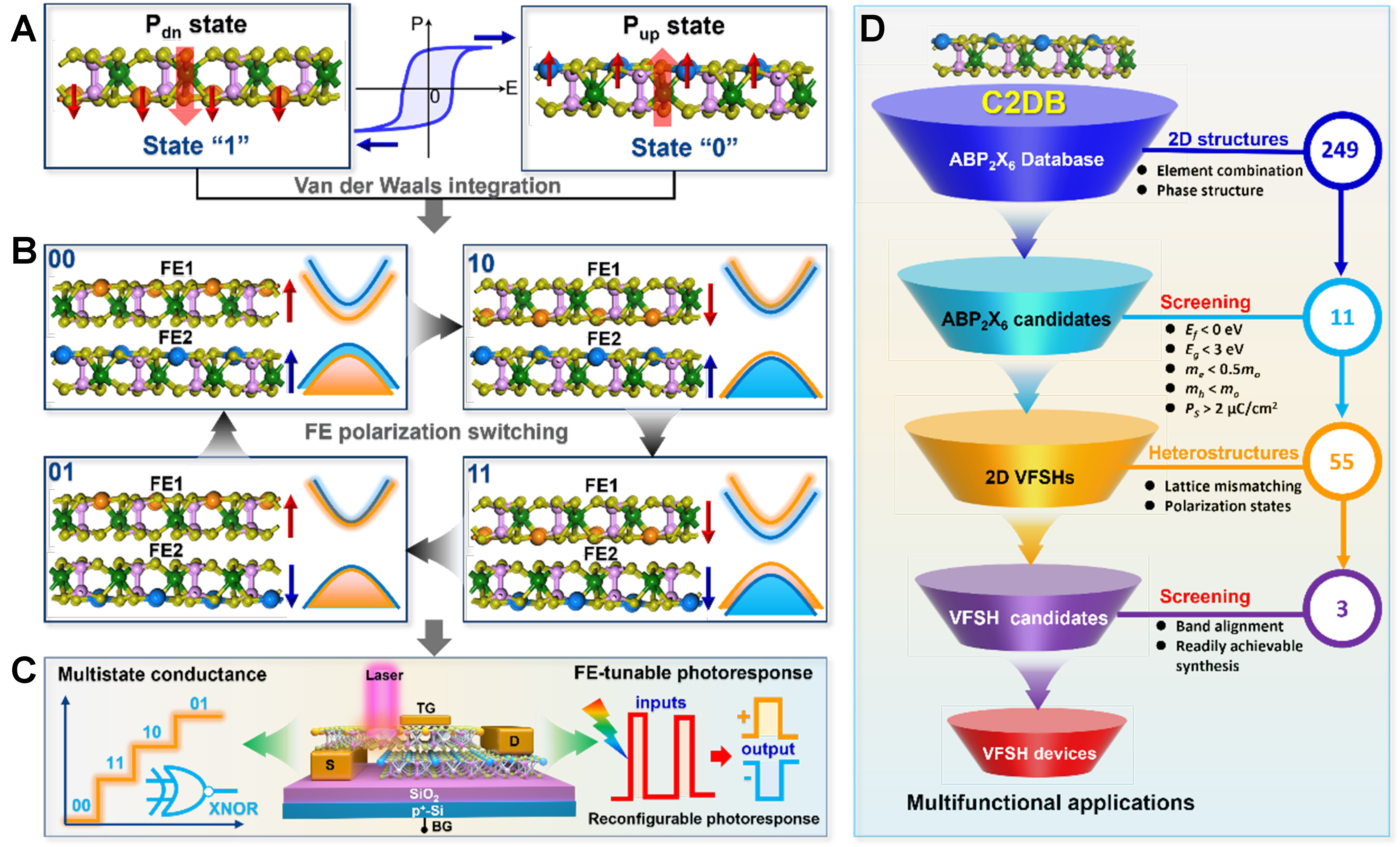
Figure 1. Basic principle and high-throughput computational screening flow of 2D ABP2X6 VFSHs for constructing all-in-one optoelectronic device architecture. (A) Atomic structure and polarization orientation of 2D ABP2X6 FE semiconductors in Pdn and Pup states; (B) FE polarization orientation and schematic band alignment of 2D ABP2X6 VFSHs in four stable polarization states (i.e., ↑↑, ↓↑, ↓↓, and ↑↓); (C) Basic concept of 2D ABP2X6 VFSH devices with FE-tunable electric and optoelectronic properties for multifunctional applications; (D) High-throughput computational screening workflow and framework of 2D ABP2X6 VFSHs for multifunctional device applications. 2D: Two-dimensional; VFSHs: vdW FE semiconductor heterojunctions; FE: ferroelectric; TG: top gate; BG: back gate; C2DB: computational 2D materials database.
Based on the FE-driven tunable electronic and optoelectronic characteristics of 2D ABP2X6 VFSHs, they can be used to construct all-in-one optoelectronic architecture for multifunctional applications, as schematically illustrated in Figure 1C. On the one hand, the band alignment of 2D VFSHs can be potentially adjusted by the control of multiple polarization states, leading to a significant modulation of the channel resistance of the VFSH device. Such a behavior enables the VFSH device to achieve in-memory logic operation. On the other hand, reversible band-alignment transition in 2D VFSHs also allows the device to switch between positive and negative photocurrents under light illumination, which facilitates the realization of optoelectronic reconfigurable logic functions in a single device. The tunable polarity and magnitude of photocurrent in the VFSH device associated with the optical intensity, wavelength, and FE polarization states can be utilized to implement in-sensor BCP for sensing images[54]. Nevertheless, the current work mainly focuses on the utilization of multiple stable polarization states to tailor the band alignment and optoelectronic properties of 2D ABP2X6 VFSHs, only offering a theoretical perspective of VFSH devices for multifunctional applications.
To find potential 2D VFSHs for the development of all-in-one device architecture, we first conducted high-throughput computational screening of highly stable ABP2X6 semiconductors with strong spontaneous polarization and superior electronic properties. The screening workflow and framework of 2D ABP2X6 VFSHs are illustrated in Figure 1D. To obtain highly stable atomically thin ABP2X6 FE semiconductors, a fundamental database including 249 initial structures is first established from C2DB[39,40]. The ABP2X6 structures are constructed by varying A-site and B-site cations and X-site anions into CuInP2S6 (or Sn2P2S6) template structure. All initial structures have been fully relaxed and then screened by the formation energy (Ef). Only the structures with negative Ef are further screened by a series of feature parameters, including the bandgaps (Eg), electron and hole carrier effective masses (me and mh), and spontaneous polarization (PS). In order to ensure that selected ABP2X6 structures are FE semiconductors with high carrier mobilities, their feature parameters need to satisfy the following conditions [Supplementary Figure 2]: (i) Eg < 3.0 eV, (ii) me < 0.5 m0 and mh < m0, (iii) PS > 2 μC/cm2. The conditions (i) and (ii) ensure that the screened structures can be considered as semiconductor channel materials with high carrier mobilities, and condition (iii) enables the selected structures to have strong FE polarization. According to the above criteria, 11 stable ABP2X6 candidates with moderate bandgaps (1.58-2.98 eV), small carrier effective masses, and strong FE polarization (> 2.56 μC/cm2) are screened. Moreover, we find that these 2D ABP2X6 candidates, typically for CuInP2S6, AgInP2S6, and AuInP2S6, do not show obvious structural distortions after the AIMD simulations for 10 ps, verifying their high thermodynamic stability (see Supplementary Figure 3 for the details). The band structures of the 11 highly stable 2D ABP2X6 candidates and their lattice, electronic, and polarization parameters are presented in Supplementary Figure 4 and Supplementary Table 4, respectively. We find that the selected ABP2X6 candidates do not include Te-based structures due to their relatively weak structural stability and small spontaneous polarization.
Based on the screened 2D ABP2X6 FE semiconductors, 55 VFSHs are created by vertically stacking two different ABP2X6 structures along the out-of-plane direction. Since the device performance and functionality of VFSHs essentially depend on their electronic structures, we first reveal the effect of FE polarization on the band alignment of 2D ABP2X6 VFSHs. For a given VFSH, it can exhibit six possible band alignments classified into three types (i.e., type I, type II, and type III), as schematically illustrated in Figure 2A. Owing to switchable polarization in the dual FE layers, ABP2X6 VFSHs exhibit at least four stable polarization states, including ↑↑, ↑↓, ↓↑, and ↓↓. Among these polarization states, the ↑↑ and ↓↓ states indicate interlayer FE coupling, while the ↑↓ and ↓↑ states exhibit interlayer AFE coupling [Supplementary Figure 1]. The polarization switching of dual FE layers in 2D VFSHs potentially induces a series of band-alignment evolutions, which offers flexibility to tailor their electronic and optoelectronic properties for multifunctional device applications.
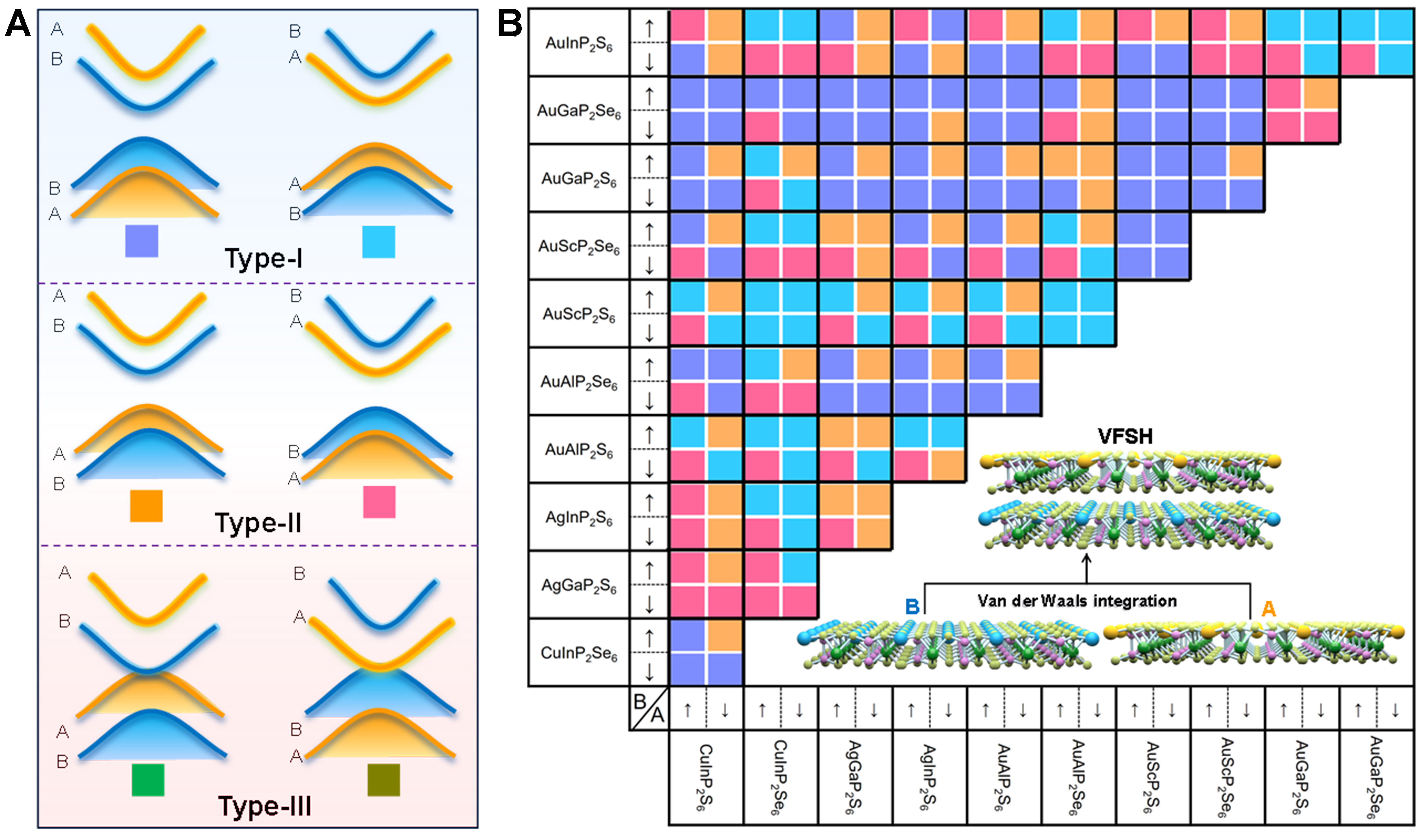
Figure 2. FE-driven band alignment transition in 2D ABP2X6 VFSHs. (A) Potential band alignment type of 2D ABP2X6 VFSHs. Here, A and B represent two different FE semiconductors in a given VFSH. Two straddling (type-I) band alignments are expressed by purple and cyan squares, and two staggered (type-II) band alignments are labeled by orange and red squares, respectively. A and B denote two different FE semiconductors in a given VFSH; (B) Predicted band alignment type of 55 2D ABP2X6 VFSHs in four stable polarization states (i.e., ↑↑, ↑↓, ↓↑, and ↓↓). The inset indicates that these VFSHs are constructed by vdW integration of two distinct 2D ABP2X6 FE semiconductors. FE: Ferroelectric; 2D: two-dimensional; VFSHs: vdW FE semiconductor heterojunctions.
To verify whether the reversible band-alignment evolution of 2D ABP2X6 VFSHs can be achieved by manipulating their polarization states, we perform DFT calculations to determine the valence band maximum (VBM) and conduction band minimum (CBM) energies (i.e., EV and EC) of 11 screened 2D FE semiconductors relative to the vacuum level [Supplementary Figure 5]. Unlike the conventional 2D semiconductors, the EV and EC of 2D FE semiconductors are completely different at two surface terminations because of the band bending induced by the polarization field[33]. This means that the polarization switching of each FE layer will potentially change the band-alignment type and band-offset values of 2D VFSHs. Based on the calculated EV and EC values, the band-alignment type of 55 2D VFSHs in four polarization states is predicted in Figure 2B. Here, the purple and cyan squares represent two type-I band alignments, and the orange and red squares denote two type-II band alignments [Figure 2A], respectively. It needs to be noted that the interlayer stacking of 2D VFSHs can potentially change the EV and EC of each FE layer in the heterojunctions due to the interface effect. However, the energy shift of EV and EC induced by the interface effect is usually not very large, so it can affect the prediction of band-offset values but scarcely change the band-offset type of 2D VFSHs. As shown in Figure 2B, the band alignment of 2D ABP2X6 VFSHs shows several important characteristics: (i) the band alignment transition in most of 2D ABP2X6 VFSHs can be driven by reversing the FE polarization states. For example, AuInP2S6/CuInP2Se6 VFSH exhibits a type-I band alignment in ↑↑ and ↑↓ states and has type-II band alignment in ↓↑, and ↓↓ states, respectively. However, the band alignment of not all of VFSHs can be changed by FE polarization switching. We find that nine VFSHs remain the type-I band alignment irrespective of FE polarization. (ii) The switching of FE polarization states can induce changes in both the bandgaps and band offsets (ΔEV and ΔEC) of all these VFSHs, regardless of band-alignment transition. For instance, AgInP2S6/CuInP2S6 VFSHs remain a type-II band alignment in
Dual-polarization-driven reversible band-alignment transition in 2D VFSHs
Based on the above screening procedures, here we choose CuInP2S6/AuInP2S6 (CIPS/AIPS) VFSHs as a prototype to evaluate the feasibility of achieving reconfigurable electronic and optoelectronic devices by the manipulation of FE polarization states. The selection of CIPS/AIPS VFSHs is derived from their small lattice mismatch (3.1%), large interfacial binding energies (-3.12~-3.78 eV), multiple reversible band-alignment transitions, and superior electronic properties. The lattice, energetic, and electronic parameters of 2D CIPS/AIPS VFSHs in four polarization states (i.e., ↑↑, ↑↓, ↓↑, and ↓↓) are listed in Supplementary Table 5. The multistate polarization switching in 2D ABP2X6 VFSHs can be experimentally achieved using a vertical dual-gate device structure. The applied top and bottom gate voltages are used to control the polarization state of the dual FE layers in either Pup or Pdn, and the polarization switching of each FE layer between Pup and Pdn states can be triggered by reversing the polarity of the top and bottom gate voltages via an intermediate paraelectric (PE) state [Supplementary Figure 7]. The transition of polarization states is inherently associated with a cooperative displacement of A- and B-site cations in the dual FE layers. The switching characteristics of multiple polarization states in CIPS/AIPS VFSHs are investigated by calculating transition energy barriers of ionic movements between any two given polarization states by using the climbing image nudged elastic band (CI-NEB) method, as shown in Figure 3A. The energy barrier for activating the transition from ↑↑ to ↑↓ state is 0.82 eV through the polarization switching of the CIPS layer from Pup to Pdn state. Then, further FE switching of the AIPS layer from Pup to Pdn state induces the transition of polarization states from ↑↓ to ↓↓, which needs to overcome an energy barrier of 0.34 eV. In contrast, the polarization switching from ↓↓ to ↑↑ needs to proceed via the AFE ↓↑ state. As shown in Figure 3A, the energy barrier is 0.21 eV for driving the transition from ↓↓ to ↓↑ and 0.34 eV for activating the transition from ↓↑ to ↑↑ state, respectively. The moderate energy barriers (0.21-0.82 eV) not only ensure the stability of these polarization states in CIPS/AIPS VFSH but also allow for the manipulation of these polarization states by the external gate-voltage modulation.
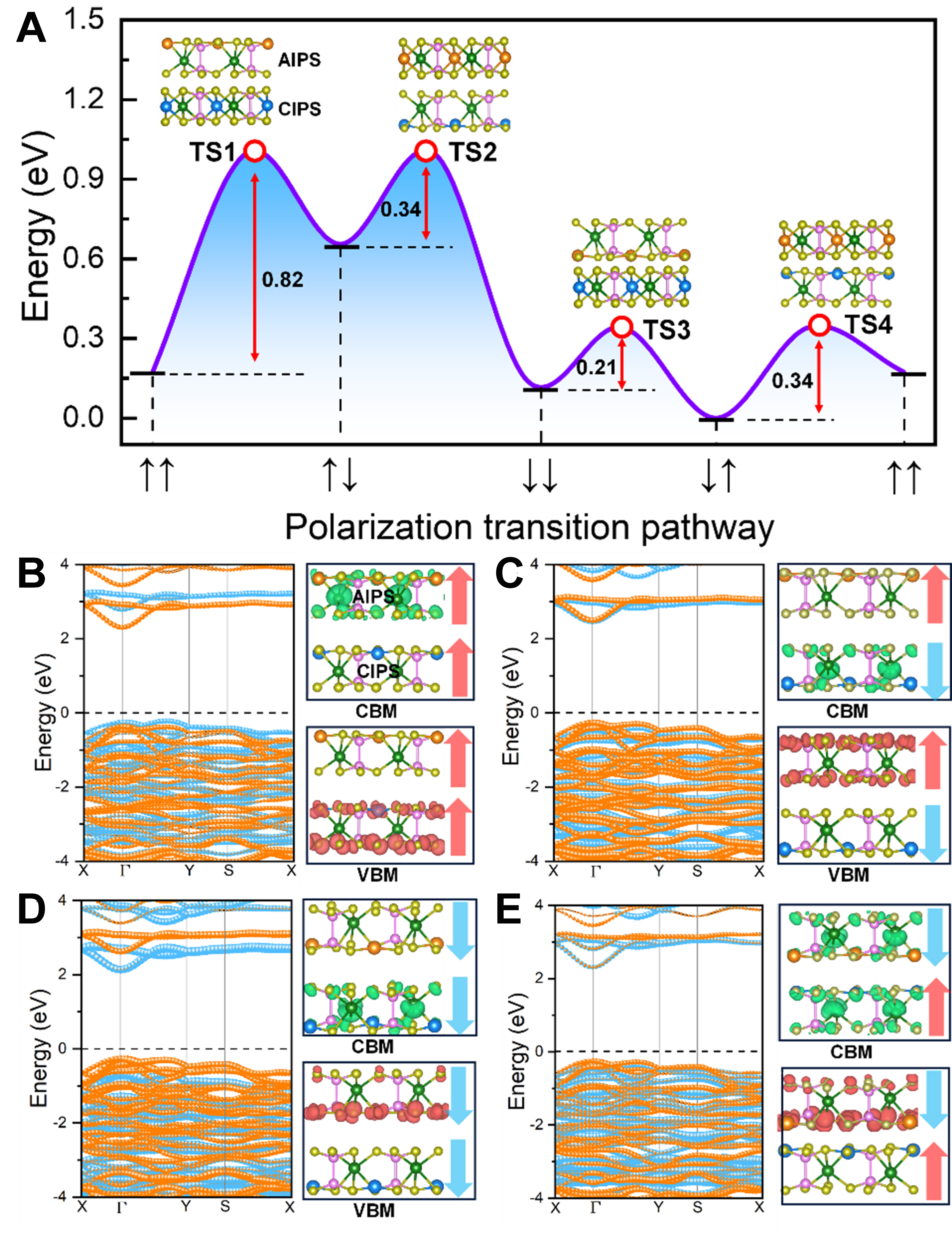
Figure 3. Polarization switching energy profile and electronic properties of 2D CIPS/AIPS VFSH in four polarization states. (A) Energy profile of FE switching among four polarization states in 2D CIPS/AIPS VFSH. TS1-TS4 denote the transition states from one polarization state to another, and the numbers correspond to the energy barriers for activating the transition of polarization states; (B-E) The projected band structure (left panel) and spatial charge-density distribution (right panel) of CBM and VBM states of CIPS/AIPS VFSH in (B) ↑↑, (C) ↑↓, (D) ↓↓, and (E) ↓↑ calculated by the HSE06 functional. The horizontal dashed line in the band structures denotes the Fermi level. The yellow and blue bands are contributed by AIPS and CIPS layers in the heterojunction, respectively. 2D: Two-dimensional; CIPS/AIPS: CuInP2S6/AuInP2S6; VFSH: vdW FE semiconductor heterojunction; FE: ferroelectric; CBM: conduction band minimum; VBM: valence band maximum.
We now turn to reveal the effect of polarization switching on electronic properties of CIPS/AIPS VFSHs. Figure 3B-E shows the projected band structures of CIPS/AIPS VFSH in four stable polarization states. The heterojunction has a type-II band alignment with a direct bandgap of 2.52 eV in the ↑↑ state. The spatial distribution of charge-density isosurfaces indicates that the CBM and VBM states are mainly contributed by AIPS and CIPS layers [Figure 3B], respectively, verifying that it is a type-II heterojunction. The transition of polarization state from ↑↑ to ↑↓ induces the band upshift of the AIPS layer and band downshift of the CIPS layer, resulting in the formation of a new type-II band alignment in the ↑↓ state [Figure 3C]. Specifically, the CBM state is mainly contributed by the CIPS layer while the VBM state is dominated by the AIPS layer, indicating a reverse carrier spatial distribution relative to the ↑↑ state. For the ↓↓ state, its band alignment is similar to that of the ↑↓ state (i.e., type II), but the conduction and valence band offsets (i.e., ΔEC and ΔEV) have been further increased compared with the band alignment of the ↑↓ state [Figure 3D], resulting in the smallest bandgap (2.40 eV). When the polarization state is switched to ↓↑, it indicates a type-I-like band alignment where the VBM state is contributed by the CIPS layer but the CBM state includes the contribution of both the CIPS and AIPS layers [Figure 3E]. In addition, we find that it remains a momentum-matched (or direct bandgap) heterojunction in all four polarization states, which contributes to high optical absorption efficiency and photoresponse.
In order to quantify the band-alignment evolution in CIPS/AIPS VFSHs, the CBM and VBM energies of the CIPS and AIPS layers in the four polarization states are presented in Figure 4A, where the polarization states evolve sequentially as ↑↑ → ↑↓ → ↓↓ (downward switching) and then ↓↓ → ↓↑ → ↑↑ (upward switching). The CBM (VBM) energy (i.e., EC and EV) of the AIPS layer firstly increases from -4.62 (-7.29) to -4.21 (-7.09) eV and the EC (EV) of the CIPS layer gradually decreases from -4.14 (-7.14) to -4.69 (-7.51) eV with a sequential switching of dual FE layers from Pup to Pdn states (i.e., from ↑↑ to ↓↓), resulting in an inversion of type-II band alignment in the VFSH. In contrast, the EC and EV of the AIPS layer decrease and those of the CIPS layer increase with a sequential switching of dual FE layers from Pdn to Pup states (i.e., from ↓↓ to ↑↑), also leading to the inversion of type-II band alignment in the VFSH. It should be noted that the intermediate ↓↑ and ↑↓ states serve as transition states connecting the two type-II alignments. In particular, the ↓↑ state exhibits the type-I-like band alignment shown in Figure 3E, in which the VBM is mainly contributed by the AIPS layer and the CBM involves contributions from both the CIPS and AIPS layers. This reversible band-alignment evolution between the two type-II states allows for the manipulation of the band edges and the spatial distributions of photogenerated carriers, which is essential for electronic and optoelectronic applications of 2D VFSHs. To understand the band alignment evolution induced by FE polarization switching, the electrostatic potential distribution (Φ) of the VFSH in different polarization states is calculated. For the VFSH in the ↑↑ state, the electrostatic potential shows an asymmetric distribution along the out-of-plane direction. Specifically, the vacuum level of CIPS termination is 0.48 eV higher than that of AIPS termination and the FE polarization points from CIPS to AIPS [Figure 4B], resulting in the band bending towards the polarization direction. Thus, the photogenerated electrons and holes can be spontaneously separated into the AIPS and CIPS layers respectively due to the existence of the built-in electric field. In contrast, for the VFSH in the ↓↓ state, the vacuum level of CIPS termination is 0.45 eV lower than that of AIPS termination [Figure 4C], enabling the FE polarization to point from AIPS to CIPS. Thanks to the band bending along the polarization direction, it shows a reverse spatial distribution of photogenerated carriers as compared to the ↑↑ state. For the ↑↓ and ↓↑ states, the VFSH exhibits the interlayer AFE configuration. Their electrostatic potentials display a nearly symmetric distribution along the out-of-plane direction due to the cancellation of the electric polarization field between the dual FE layers [Figure 4D and Supplementary Figure 8], resulting in smaller band bending in both the ↑↓ and ↓↑ states. Hence, a sequential switching of polarization states from ↑↑, ↑↓, to ↓↓ induces the band upshift of the AIPS layer and the band downshift of the CIPS layer [Figure 4E], while the FE polarization switching from ↓↓, ↓↑, to ↑↑ leads to a reverse band shift of the dual FE layers [Supplementary Figure 9]. Such a result confirms that the sequential polarization switching leads to a reversible type-II band alignment transition in the VFSH.
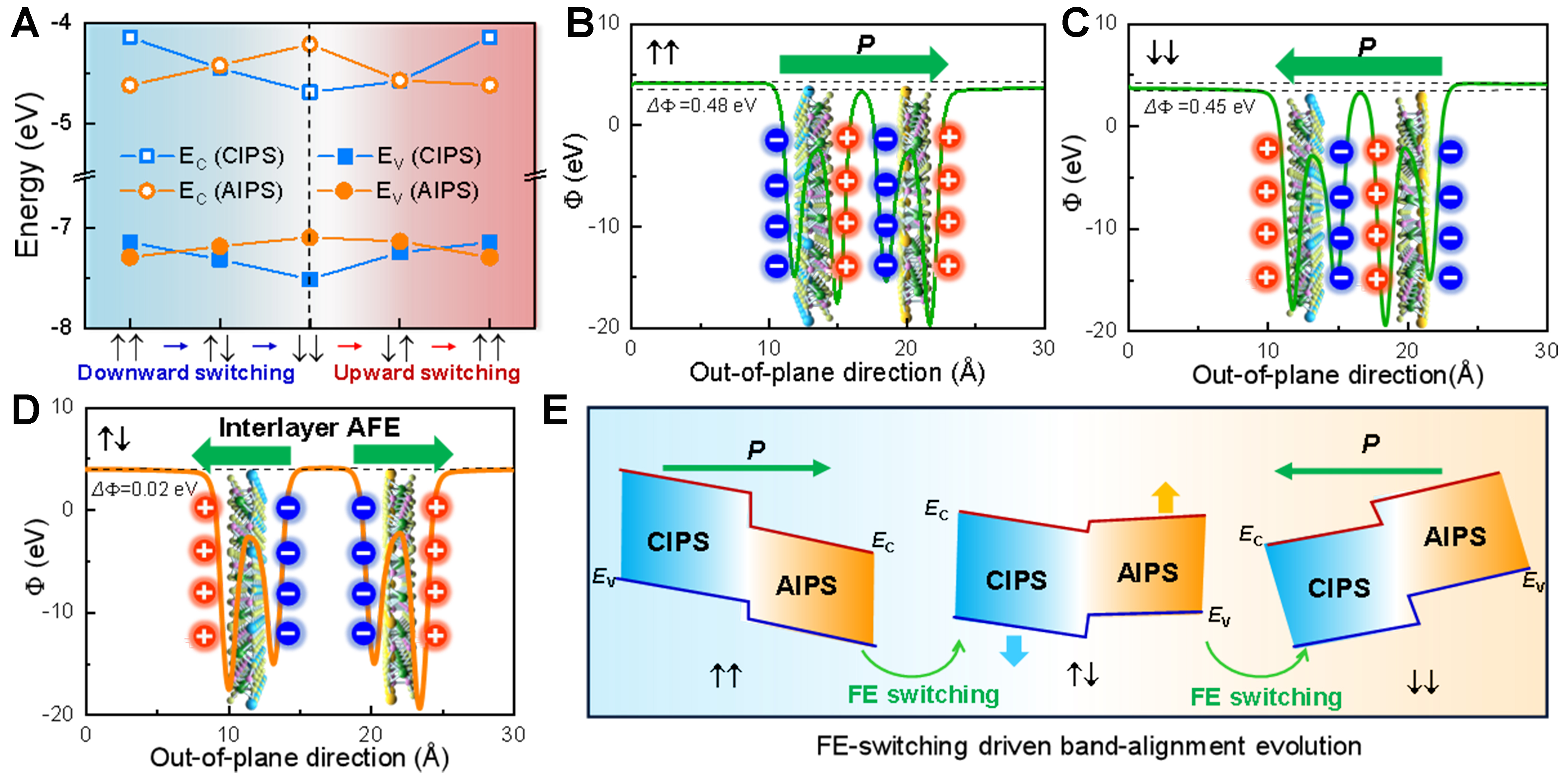
Figure 4. FE polarization effect on the band alignment evolution of 2D CIPS/AIPS VFSH. (A) The variation of EC and EV of CIPS and AIPS layers in the VFSH with the sequential switching of four polarization states; (B-D) Electrostatic potential distribution of CIPS/AIPS VFSH at (B) ↑↑ state, (C) ↓↓ state, and (D) ↑↓ state. The ↑↑ and ↓↓ states correspond to interlayer FE coupling, and ↑↓ and ↓↑ states correspond to interlayer AFE coupling. The arrows denote the polarization direction; (E) The band-alignment evolution in CIPS/AIPS VFSH driven by the switching of polarization states from ↑↑, ↑↓, to ↓↓ state. FE: Ferroelectric; 2D: two-dimensional; CIPS/AIPS: CuInP2S6/AuInP2S6; VFSH: vdW FE semiconductor heterojunction; AFE: antiferroelectric.
In addition to the manipulation of band alignment, the optical absorption ability of 2D VFSHs is also important for evaluating their potential in optoelectronic applications. The absorption spectra and optical absorptivity of CIPS/AIPS VFSH are presented in Supplementary Figure 10. The optical properties of independent CIPS and AIPS monolayers are also calculated for comparison. The absorption coefficients of VFSH in all polarization states are 105-106 cm-1 from the visible (VIS) to the ultraviolet (UV) region and the maximum absorptivity arrives at ~30%, which are nearly two times larger than those of the freestanding CIPS and AIPS monolayers. This means that the formation of 2D VFSHs contributes to the promotion of optical absorption efficiency. Meanwhile, we find that the absorption coefficients and photoresponse range of CIPS/AIPS VFSH in four polarization states are very close. However, the four polarization states yield different band alignments that alter the spatial distribution of photogenerated carriers upon polarization switching, which enables the polarity-tunable photocurrent in VFSH devices. Such a result will be discussed later.
Electronic transport and logic function in 2D CIPS/AIPS device
The FE polarization effect on the electrical transport of CIPS/AIPS VFSH is studied by using a transistor model in which the heterojunction is used as the channel and the four polarization states can be manipulated by loading bottom/top gate voltages through the piezoelectric force microscopy (PFM) tip in experiment, as schematically illustrated in Figure 5A. Here, quantum transport simulations are performed using the NEGF method within the DFT framework (see the Methods section for details). Figure 5B shows the output characteristic (I-V) curves of CIPS/AIPS VFSH devices in four polarization states. The output current (Ids) of the device in all polarization states rises with increasing bias voltage (Vds). It can be found that there exists a threshold voltage (Vth) in all polarization states due to their type-II (or type-I) band-alignment nature. Interestingly, the Ids of two FE states (i.e., ↑↑ and ↓↓) is far larger than that of two AFE states (↑↓ and ↓↑) when Vds is beyond 1.2 V. For instance, the Ids of the ↑↑ and ↓↓ states arrives at 620-750 nA, while the Ids of the ↑↓ and ↓↑ states is only 100-200 nA at Vds = 2 V. The large discrepancy of Ids can be understood by the transmission spectra of the VFSH device, as shown in Figure 5C. The transmission coefficients of two FE states are notably larger than those of two AFE states, which benefits from the polarization-induced band bending that facilitates electron tunneling via available conduction channels[33]. Hence, the large Ids of two FE states makes the device operate in a low resistance state (LRS), while the smaller Ids of two AFE states corresponds to the device at a high resistance state (HRS). Considering the polarization states manipulated by the top and bottom gate voltages (VTG and VBG), the switching between HRS and LRS in the device can be achieved by alternating positive and negative VTG and VBG.
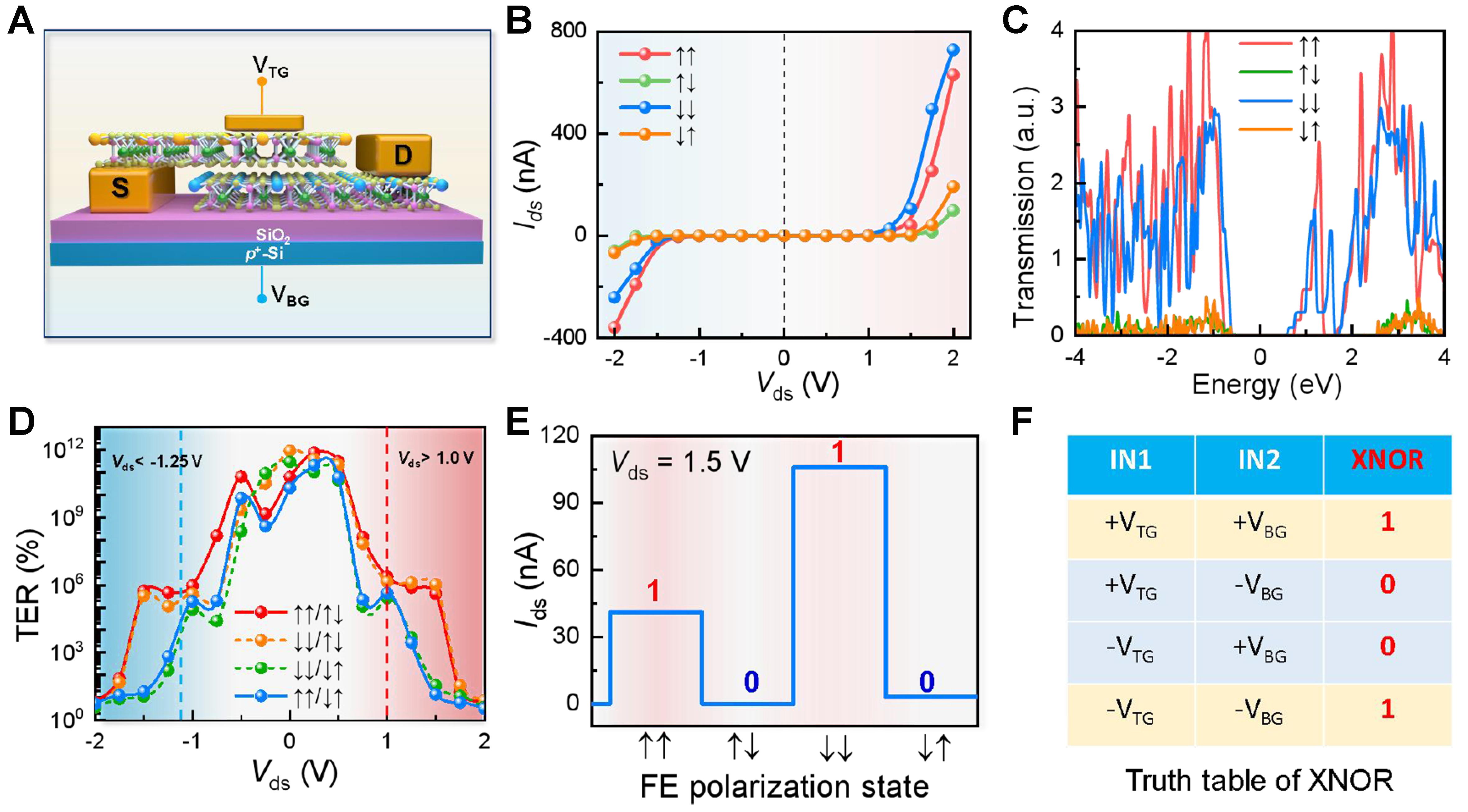
Figure 5. Effect of multiple polarization states on electrical transport of CIPS/AIPS VFSH device. (A) Schematic diagram of CIPS/AIPS transistor structure; (B) Ids-Vds curves of CIPS/AIPS device in four polarization states; (C) Transmission spectra of CIPS/AIPS device in four polarization states; (D) TER of CIPS/AIPS device as a function of Vds; (E) Ids of CIPS/AIPS device in four polarization states at Vds = 1.5 V. The Ids of four polarization states is larger than 10 nA as the logic output “1” and lower than 10 nA as the logic output “0”; (F) Truth table of XNOR logic operation. Here +VTG and +VBG represent logic input “1”, and -VTG and -VBG represent logic input “0”. CIPS/AIPS: CuInP2S6/AuInP2S6; VFSH: vdW FE semiconductor heterojunction; TER: tunneling electroresistance ratio.
Owing to the large discrepancy in the output current between the FE and AFE states, the device exhibits a large TER ratio, as shown in Figure 5D. It should be emphasized that the TER values are ideal estimates from DFT-based quantum transport calculations. The ultrahigh TER values (108%-1012%) obtained at small bias voltages (-1 V < Vds < 1 V) mainly arise from the large difference in the near-zero off-state current between the FE and AFE states, which is associated with a relatively large bandgap of the VFSH (≥ 2.4 eV). Therefore, these ultrahigh TER values have little practical significance because of ultralow output current (Ids < 1 nA). In order to ensure the device functionality, the VFSH device needs to work at a relatively larger Vds. Typically, for 1 V < Vds < 1.5 V, the device operates with a moderate output current in the ↑↑ and ↓↓ states (Ids > 1 nA) and simultaneously exhibits relatively large TER values (~106%) between the ↓↓ and ↑↓ states at the bias voltage of 1.5 V, enabling the realization of device logic functions. Figure 5E shows the Ids of CIPS/AIPS devices in four polarization states at Vds = 1.5 V. The Ids of the device is 41, 0.01, 106, and 3 nA for ↑↑, ↑↓, ↓↓, and ↓↑ states, respectively. Using 10 nA as a benchmark, the Ids is beyond the threshold value (i.e., Ith = 10 nA) as the logic output “1” and smaller than Ith as the logic output “0”. Thus, the VFSH device can be used to perform XNOR logic gate using VTG and VBG as the input ports with the sequence of 0-0, 1-0, 0-1, and 1-1, and the corresponding truth table for the XNOR gate operation is shown in Figure 5F. Here, the positive gate voltages (i.e., +VTG and +VBG) are defined as the logic input “1”, and the negative gate voltages (i.e., -VTG and
Photoresponse and optoelectronic logic operations in 2D CIPS/AIPS devices
The FE polarization effect on optoelectronic characteristics of 2D CIPS/AIPS devices is explored using a photodetector model in which light illumination on the VFSH induces the photocurrent through the photogalvanic effect (PGE), as schematically displayed in Figure 6A. Here, the device photocurrent is calculated by using the DFT framework combined with NEGF formalism (see the Methods section for details). The generation of photocurrent in semiconductor materials induced by the PGE is usually associated with their non-centrosymmetric structures. For CIPS/AIPS VFSHs, the polarization-induced built-in electric field can further amplify the PGE because of spontaneous separation of photogenerated electron–hole pairs driven by the built-in electric field, resulting in the generation of a finite photocurrent in the VFSH device without external bias voltage. As mentioned above, reversible type-II band-alignment transition in CIPS/AIPS devices has been demonstrated by the switching of polarization state from ↑↑ to ↓↓, resulting in a reverse distribution of photogenerated carriers in two polarization states [Figure 6B and C]. Such a characteristic allows for achieving reconfigurable photoresponse and optoelectronic logic functions via the utilization of polarity-tunable photocurrent in 2D CIPS/AIPS devices.
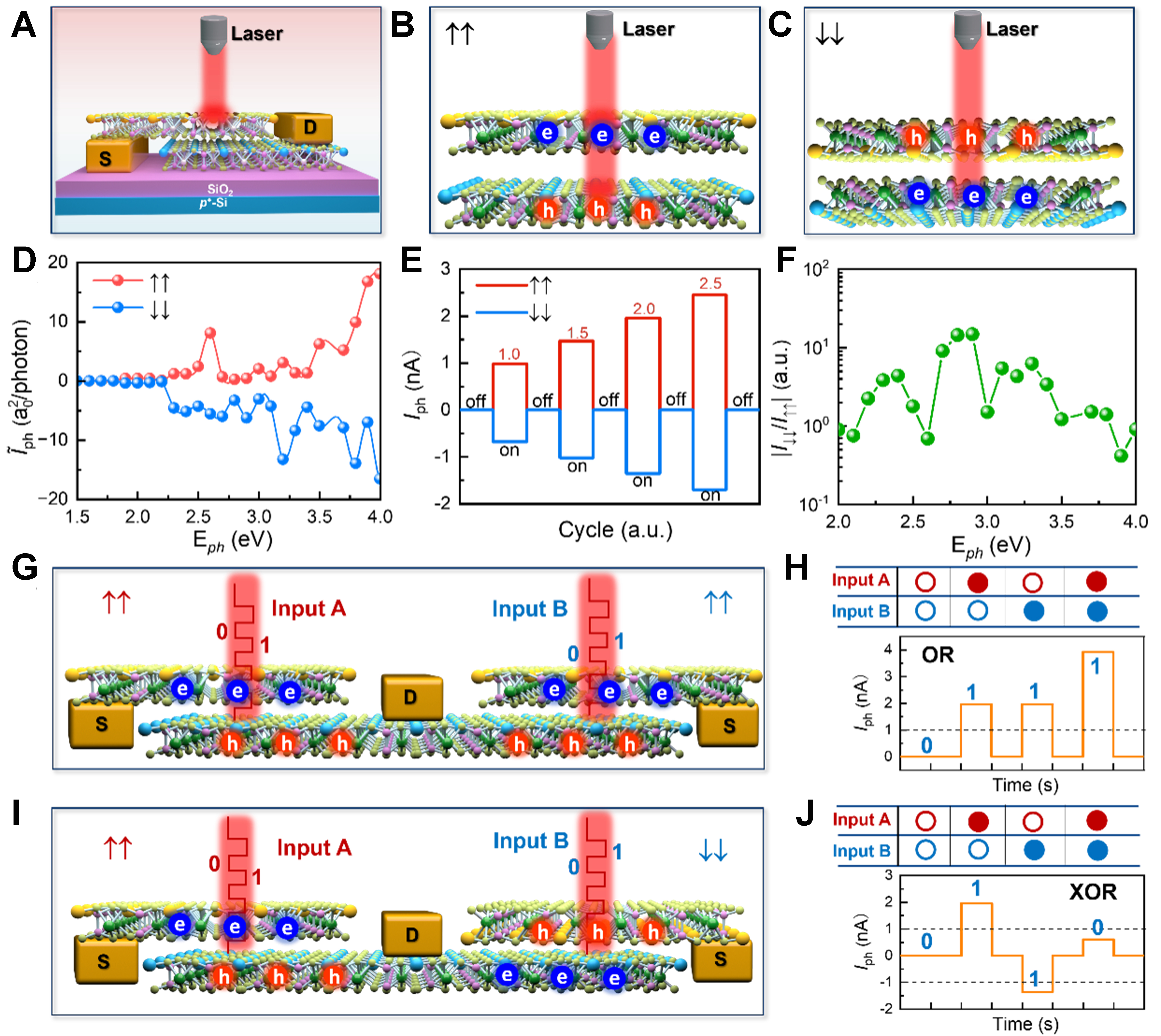
Figure 6. FE-dependent photoresponse and optoelectronic logic functions of CIPS/AIPS VFSH device. (A) Schematic diagram of a CIPS/AIPS photodetector; (B and C) Laser-induced carrier spatial distribution of CIPS/AIPS device in ↑↑ and ↓↓ states; (D) Normalized photocurrent (
Figure 6D shows the normalized photocurrent (
In addition to implementing in-sensor BCP applications, the reconfigurable positive and negative photoresponse can also be utilized to achieve complex optoelectronic logic operations. The optoelectronic logic gates are realized on the basis of a complementary CIPS/AIPS phototransistor consisting of a center drain and bilateral sources [Figure 6G], which actually includes two VFSH devices and two optical input terminations (i.e., A and B). The input light and polarization state of the VFSH are used to control the magnitude and polarity of photocurrent. Here, the logic input “0” represents the light-off state and the logic input “1” denotes the light-on state under the specified photon energy and optical intensity. The logic output is defined by the magnitude of the output photocurrent. More specifically, the logic output “0” corresponds to |Iph| < 1 nA and the logic output “1” corresponds to |Iph| ≥ 1 nA. Typically, for the polarization state of two VFSH devices in the ↑↑ state with Eph = 2.6 eV and Pin = 2.0 W/m2, the two optical terminations A-B with the input sequence of 0-0, 1-0, 0-1, and 1-1 induce an output sequence of 0, 1, 1, 1 [Figure 6H], which acts as an OR logic gate. Similarly, tuning the polarization state of the two VFSH devices in the ↓↓ state with Eph =
CONCLUSIONS
In summary, we reported an efficient strategy to achieve reconfigurable band alignment and positive/negative photoresponse in 2D VFSHs for an all-in-one optoelectronic device architecture by coupling nonvolatile dual-FE polarization fields. Our calculated results revealed that switchable dual FE polarization layers in 2D ABP2X6 VFSHs induce at least four stable polarization states, creating a large degree of freedom to modulate their band alignment, electrical transport, and photoresponse. Taking 2D CIPS/AIPS VFSHs as a prototype example, we demonstrated a reversible band-alignment evolution between two type-II states via an intermediate type-I-like state (↓↑) induced by switching the dual FE polarization field, giving rise to a notable difference of output current among four stable polarization states. This enables the VFSH device to achieve a theoretical TER of 106% between ↓↓ and ↑↓ states at the bias voltage of 1.5 V, allowing the realization of complex logic functions. The reverse type-II band alignment between two FE states enables the VFSH device to switch between positive and negative photocurrents, which can be utilized to achieve multiple optoelectronic logic operations including OR, AND, and XOR in a single device. Moreover, the tunable positive and negative photoresponse of the VFSH device can also be used to implement in-sensor convolutional processing (BCP) for sensing images. This work opens up a new route to realize band-alignment engineering in ABP2X6 VFSHs for the development of all-in-one optoelectronic device architecture.
DECLARATIONS
Acknowledgments
Computational support from the HZWTECH cloud computing platform is acknowledged. The quantum transport calculations in this work were performed using the Nanodcal package on the HZWTECH platform.
Authors’ contributions
Conception and design of the study and methodology: Xie, D.; Cao, D.; Shu, H.
Data analysis and interpretation: Xie, D.; Liu, Z.; Wang, J.
Data visualization and manuscript drafting: Xie, D.; Liu, Z.; Wang, J.; Shu, H.
Project administration and coordination: Cao, D.; Shu, H.
Resources and experimental support: Cao, D.; Chen, X.; Shu, H.
Supervision and scientific guidance: Chen, X.; Shu, H.
Manuscript review, editing, and critical revision: Xie, D.; Cao, D.; Chen, X.; Shu, H.
All authors read and approved the final manuscript.
Availability of data and materials
The datasets generated and analyzed during the current study are presented as figures and tables in the main text and Supplementary Materials and are available from the corresponding authors upon reasonable request.
AI and AI-assisted tools statement
Not applicable.
Financial support and sponsorship
This work was supported by the National Natural Science Foundation of China (Grant No. 62174151), the Fund of Zhejiang Provincial Natural Science Foundation of China (Grant No. LZ22F040003), Fundamental Research Funds for the Provincial Universities of Zhejiang (Grant No. 2026YW100), and Open Fund of State Key Laboratory of Infrared Physics (Grant No. SITP-NLIST-YB-2024-09).
Conflicts of interest
All authors declared that there are no conflicts of interest.
Ethical approval and consent to participate
Not applicable.
Consent for publication
Not applicable.
Copyright
© The Author(s) 2026.
Supplementary Materials
REFERENCES
2. Guo, L.; Sun, H.; Yang, S.; et al. High-precision in-sensor computing reaching up to 10 bits. Adv. Mater. 2026, 38, e19096.
3. Tang, H.; Yu, N.; Min, P.; Guo, R.; Zhang, G. In-sensor-memory computing for post-von neumann intelligence: a perspective. Nanomicro. Lett. 2026, 18, 338.
4. Liu, C.; Chen, H.; Wang, S.; et al. Two-dimensional materials for next-generation computing technologies. Nat. Nanotechnol. 2020, 15, 545-57.
5. Seo, S.; Jo, S. H.; Kim, S.; et al. Artificial optic-neural synapse for colored and color-mixed pattern recognition. Nat. Commun. 2018, 9, 5106.
6. Cui, D.; Pei, M.; Lin, Z.; et al. Versatile optoelectronic memristor based on wide-bandgap Ga2O3 for artificial synapses and neuromorphic computing. Light. Sci. Appl. 2025, 14, 161.
7. Wu, G.; Zhang, X.; Feng, G.; et al. Ferroelectric-defined reconfigurable homojunctions for in-memory sensing and computing. Nat. Mater. 2023, 22, 1499-506.
8. Sun, X.; Wang, D.; Wu, X.; et al. Facile formation of van der Waals metal contact with III-nitride semiconductors. Sci. Bull. 2024, 69, 3692-9.
9. Sun, H.; Qian, L.; Hong, X.; et al. Hardware-intrinsic encrypted imaging and neuromorphic computing enabled by bias-reconfigurable AlScN/GaN heterojunction ultraviolet photodetector. Adv. Photon. 2025, 7, 1-11.
10. Li, M. Y.; Shi, Y.; Cheng, C. C.; et al. NANOELECTRONICS. Epitaxial growth of a monolayer WSe2-MoS2 lateral p-n junction with an atomically sharp interface. Science 2015, 349, 524-8.
11. Lu, Y.; Xie, D.; Zhang, C.; Cao, D.; Chen, X.; Shu, H. Band alignment engineering in 2D ferroelectric van der Waals heterostructures for all‐in‐one optoelectronic architecture. Adv. Elect. Mater. 2025, 11, 2400269.
12. Bu, Y.; Ye, T.; Wang, R.; et al. High discrimination infrared polarimetry via intrinsic anisotropic photogating in black phosphorus meta-polarization detectors. Nat. Commun. 2025, 16, 10137.
13. Liu, Y.; Weiss, N. O.; Duan, X.; Cheng, H.; Huang, Y.; Duan, X. Van der Waals heterostructures and devices. Nat. Rev. Mater. 2016, 1, 16042.
14. Wu, S.; Deng, J.; Wang, X.; et al. Polarization photodetectors with configurable polarity transition enabled by programmable ferroelectric-doping patterns. Nat. Commun. 2024, 15, 8743.
15. Chen, Y.; Tan, C.; Wang, Z.; et al. Momentum-matching and band-alignment van der Waals heterostructures for high-efficiency infrared photodetection. Sci. Adv. 2022, 8, eabq1781.
16. Wang, C. Y.; Liang, S. J.; Wang, S.; et al. Gate-tunable van der Waals heterostructure for reconfigurable neural network vision sensor. Sci. Adv. 2020, 6, eaba6173.
17. Kistner-Morris, J.; Shi, A.; Liu, E.; et al. Electric-field tunable type-I to type-II band alignment transition in MoSe2/WS2 heterobilayers. Nat. Commun. 2024, 15, 4075.
18. Huang, H.; Shi, S.; Zha, J.; et al. In-sensor compressing via programmable optoelectronic sensors based on van der Waals heterostructures for intelligent machine vision. Nat. Commun. 2025, 16, 3836.
19. Quan, H.; Ma, C.; Wu, M.; et al. Bioinspired multi-dimensional convolution kernels enabled by gate-programmable NiTe2/WSe2 nanostrip photodetector. Matter 2026, 9, 102751.
20. Chen, J. W.; Lo, S. T.; Ho, S. C.; et al. A gate-free monolayer WSe2 pn diode. Nat. Commun. 2018, 9, 3143.
21. Kamaei, S.; Liu, X.; Saeidi, A.; et al. Ferroelectric gating of two-dimensional semiconductors for the integration of steep-slope logic and neuromorphic devices. Nat. Electron. 2023, 6, 658-68.
22. Chen, Y.; Wang, X.; Huang, L.; et al. Ferroelectric-tuned van der Waals heterojunction with band alignment evolution. Nat. Commun. 2021, 12, 4030.
23. Dawber, M.; Rabe, K. M.; Scott, J. F. Physics of thin-film ferroelectric oxides. Rev. Mod. Phys. 2005, 77, 1083-130.
24. Spaldin, N. A. Materials science. Fundamental size limits in ferroelectricity. Science 2004, 304, 1606-7.
25. Chen, C.; Zhou, Y.; Tong, L.; Pang, Y.; Xu, J. Emerging 2D ferroelectric devices for in-sensor and in-memory computing. Adv. Mater. 2025, 37, e2400332.
26. Wang, C.; You, L.; Cobden, D.; Wang, J. Towards two-dimensional van der Waals ferroelectrics. Nat. Mater. 2023, 22, 542-52.
27. Li, Y.; Fu, J.; Mao, X.; et al. Enhanced bulk photovoltaic effect in two-dimensional ferroelectric CuInP2S6. Nat. Commun. 2021, 12, 5896.
28. Liu, F.; You, L.; Seyler, K. L.; et al. Room-temperature ferroelectricity in CuInP2S6 ultrathin flakes. Nat. Commun. 2016, 7, 12357.
29. Zhao, M.; Gou, G.; Ding, X.; Sun, J. An ultrathin two-dimensional vertical ferroelectric tunneling junction based on CuInP2S6 monolayer. Nanoscale 2020, 12, 12522-30.
30. Men, M.; Deng, Z.; Zhao, Z.; et al. Polarization-modulated programmable photovoltaic performance of a designed ferroelectric heterojunction. Nat. Commun. 2026, 17, 2096.
31. Shen, Z.; Li, A.; Wang, Q.; et al. Full‐vdW heterosynaptic memtransistor with the ferroelectric inserted functional layer and its neuromorphic applications. Adv. Funct. Mater. 2025, 35, 2412832.
32. Zhou, Y.; Li, S.; Li, X.; et al. Reconfigurable ferroelectric heterostructure device for self‐powered broadband sensing, spectral tuning, and optoelectronic synapse. Adv. Funct. Mater. 2026, 36, e76109.
33. Zhang, C.; Xie, D.; Liu, Z.; et al. Reconfigurable symmetry-broken van der Waals ferroelectric semiconductor heterojunctions for all-in-one optoelectronic devices. ACS. Nano. 2025, 19, 42928-40.
34. Ding, J.; Cheng, R.; Hou, Y.; et al. Reconfigurable van der Waals ferroionic barristor for multifunctional nanoelectronics. Adv. Funct. Mater. 2024, 34, 2407694.
35. Chen, M.; Qi, L.; Zhou, L.; et al. Ferroelectrically‐controlled multi‐state switching in AgVP2S6/WSe2 van der Waals heterojunctions for efficient visible‐to‐near‐infrared photodetection. Adv. Opt. Mater. 2025, 13, e01644.
36. Singh, P.; Baek, S.; Yoo, H. H.; Niu, J.; Park, J. H.; Lee, S. Two-dimensional CIPS-InSe van der Waal heterostructure ferroelectric field effect transistor for nonvolatile memory applications. ACS. Nano. 2022, 16, 5418-26.
37. Zhang, D.; Schoenherr, P.; Sharma, P.; Seidel, J. Ferroelectric order in van der Waals layered materials. Nat. Rev. Mater. 2023, 8, 25-40.
38. Tan, Y.; Zheng, J.; Niu, X.; et al. Research progress on 2D ferroelectric and ferrovalley materials and their neuromorphic application. Sci. China. Phys. Mech. Astron. 2023, 66, 2055.
39. Haastrup, S.; Strange, M.; Pandey, M.; et al. The computational 2D materials database: high-throughput modeling and discovery of atomically thin crystals. 2D. Mater. 2018, 5, 042002.
40. Gjerding, M. N.; Taghizadeh, A.; Rasmussen, A.; et al. Recent progress of the computational 2D materials database (C2DB). 2D. Mater. 2021, 8, 044002.
41. Kresse, G.; Furthmüller, J. Efficient iterative schemes for ab initio total-energy calculations using a plane-wave basis set. Phys. Rev. B. Condens. Matter. 1996, 54, 11169-86.
42. Blöchl, P. E. Projector augmented-wave method. Phys. Rev. B. Condens. Matter. 1994, 50, 17953-79.
43. Kresse, G.; Joubert, D. From ultrasoft pseudopotentials to the projector augmented-wave method. Phys. Rev. B. 1999, 59, 1758-75.
44. Payne, M. C.; Teter, M. P.; Allan, D. C.; Arias, T. A.; Joannopoulos, J. D. Iterative minimization techniques for ab initio total-energy calculations: molecular dynamics and conjugate gradients. Rev. Mod. Phys. 1992, 64, 1045.
45. Grimme, S.; Antony, J.; Ehrlich, S.; Krieg, H. A consistent and accurate ab initio parametrization of density functional dispersion correction (DFT-D) for the 94 elements H-Pu. J. Chem. Phys. 2010, 132, 154104.
46. Henkelman, G.; Uberuaga, B. P.; Jónsson, H. A climbing image nudged elastic band method for finding saddle points and minimum energy paths. J. Chem. Phys. 2000, 113, 9901-4.
47. King-Smith, R. D.; Vanderbilt, D. Theory of polarization of crystalline solids. Phys. Rev. B. Condens. Matter. 1993, 47, 1651-4.
48. Krukau, A. V.; Vydrov, O. A.; Izmaylov, A. F.; Scuseria, G. E. Influence of the exchange screening parameter on the performance of screened hybrid functionals. J. Chem. Phys. 2006, 125, 224106.
49. Taylor, J.; Guo, H.; Wang, J. Ab initio modeling of quantum transport properties of molecular electronic devices. Phys. Rev. B. 2001, 63, 245407.
50. Soler, J. M.; Artacho, E.; Gale, J. D.; et al. The SIESTA method for ab initio order-N materials simulation. J. Phys. Condens. Matter. 2002, 14, 2745.
51. Meir, Y.; Wingreen, N. S. Landauer formula for the current through an interacting electron region. Phys. Rev. Lett. 1992, 68, 2512-5.
52. Xie, Y.; Zhang, L.; Zhu, Y.; Liu, L.; Guo, H. Photogalvanic effect in monolayer black phosphorus. Nanotechnology 2015, 26, 455202.
53. Que, H.; Li, B.; Sun, L.; et al. Synthesis of two-dimensional transition metal phosphorous chalcogenides and their high-entropy alloys. Nat. Synth. 2025, 4, 582-91.
54. Pi, L.; Wang, P.; Liang, S.; et al. Broadband convolutional processing using band-alignment-tunable heterostructures. Nat. Electron. 2022, 5, 248-54.
Cite This Article
 Open Access
How to Cite
Xie, D.; Liu, Z.; Wang, J.; Cao, D.; Chen, X.; Shu, H. Computational screening of reconfigurable van der Waals ferroelectric semiconductor heterojunctions for all-in-one optoelectronic devices. J. Mater. Inf. 2026, 6, 50. https://dx.doi.org/10.20517/jmi.2026.70
Download Citation
Export Citation File:
Type of Import
Tips on Downloading Citation
Citation Manager File Format
Type of Import
Direct Import: When the Direct Import option is selected (the default state), a dialogue box will give you the option to Save or Open the downloaded citation data. Choosing Open will either launch your citation manager or give you a choice of applications with which to use the metadata. The Save option saves the file locally for later use.
Indirect Import: When the Indirect Import option is selected, the metadata is displayed and may be copied and pasted as needed.
About This Article
Copyright

Data & Comments
Data
0







Comments
Comments must be written in English. Spam, offensive content, impersonation, and private information will not be permitted. If any comment is reported and identified as inappropriate content by OAE staff, the comment will be removed without notice. If you have any queries or need any help, please contact us at support@oaepublish.com.