

fig7
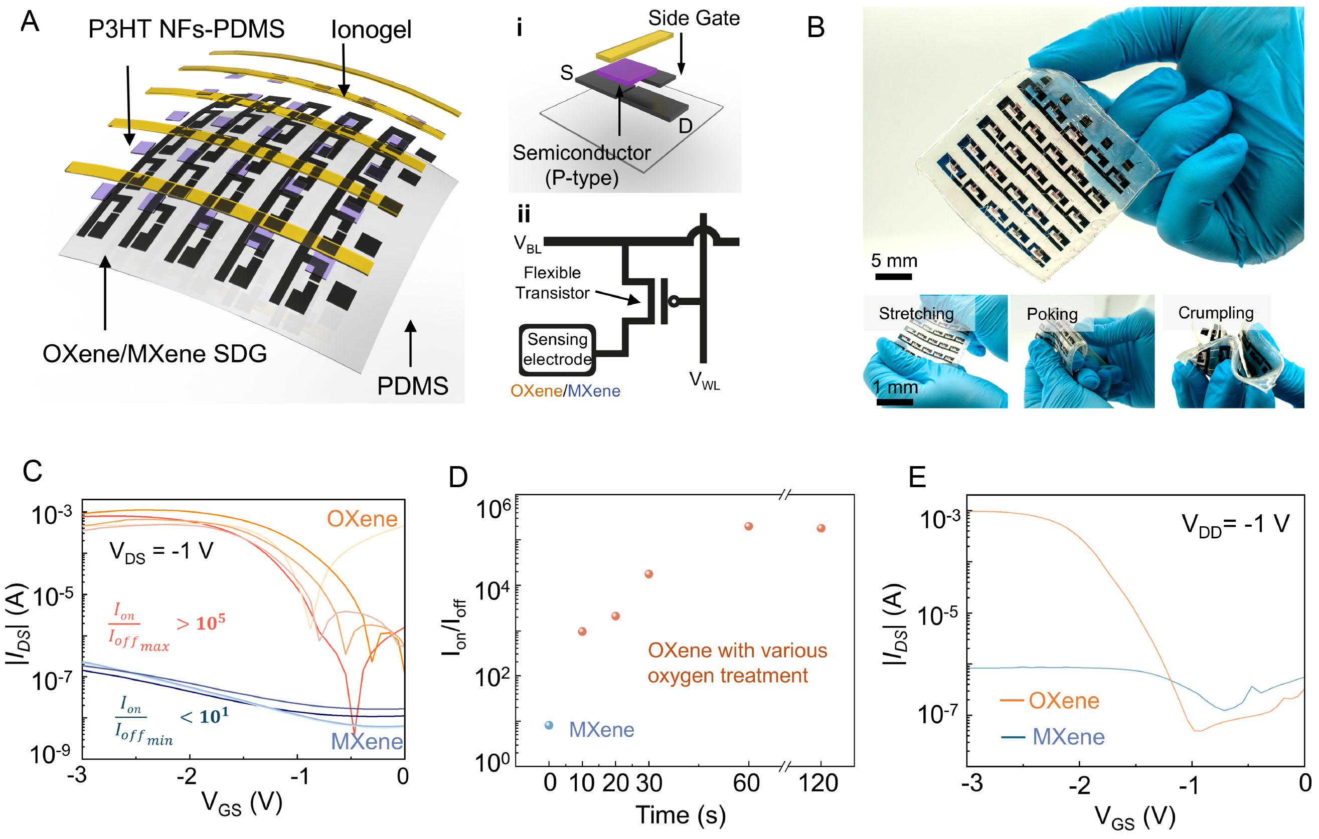
Figure 7. Symmetry engineering in OXene enables reconfigurable “0” and “1” logic interfaces as SDG layers in flexible transistor arrays. (A) An exploded schematic view of the 5 × 5 transistor array with OXene/MXene SDG layer. The constituent components include flexible Polydimethylsiloxane (PDMS, 1:10) substrates, OXene or MXene traces serve as transistor interconnects, with poly(3-hexylthiophene-2,5-diyl) nanofibrils-PDMS (labeled as P3HT NFs-PDMS) as the semiconductor, and ionogel as the flexible dielectric layer. (i) Schematic exploded view of the architecture of a transistor node; (ii) The circuit diagram for a single sensory transistor in the active matrix; (B) Optical image of transistor array under various mechanical deformations; (C) Representative transfer characteristics of the OXene/MXene transistors with a p-type P3HT NFs-PDMS semiconductor layer. The gate current, which ranged around 10-10 ~ 10-11 A, is omitted. Distinct OXene curves are attributed to different oxygen plasma treatment periods (30 cc min-1, power 200W 40 KHz, ranging from 10 s to 120 s); (D) Switching current ratios (Ion/Ioff) of OXene transistors under various oxygen treatment periods, in comparison to MXene transistors without oxygen treatment; (E) Transfer characteristics of one pressure-sensitive pixel in the active matrix with OXene or MXene SDG layer. (A-E) are reproduced as cropped excerpts from ref.[187], under the CC BY-NC-ND 4.0 license; the depicted content of the individual panels was not altered. SDG: Source-drain-gate layer; PDMS: polydimethylsiloxane; VBL: bit line voltage; VWL: word line voltage; IDS: drain-source current; VDS: drain-source voltage; VGS: gate-source voltage; NF: nanofibril.