
fig6
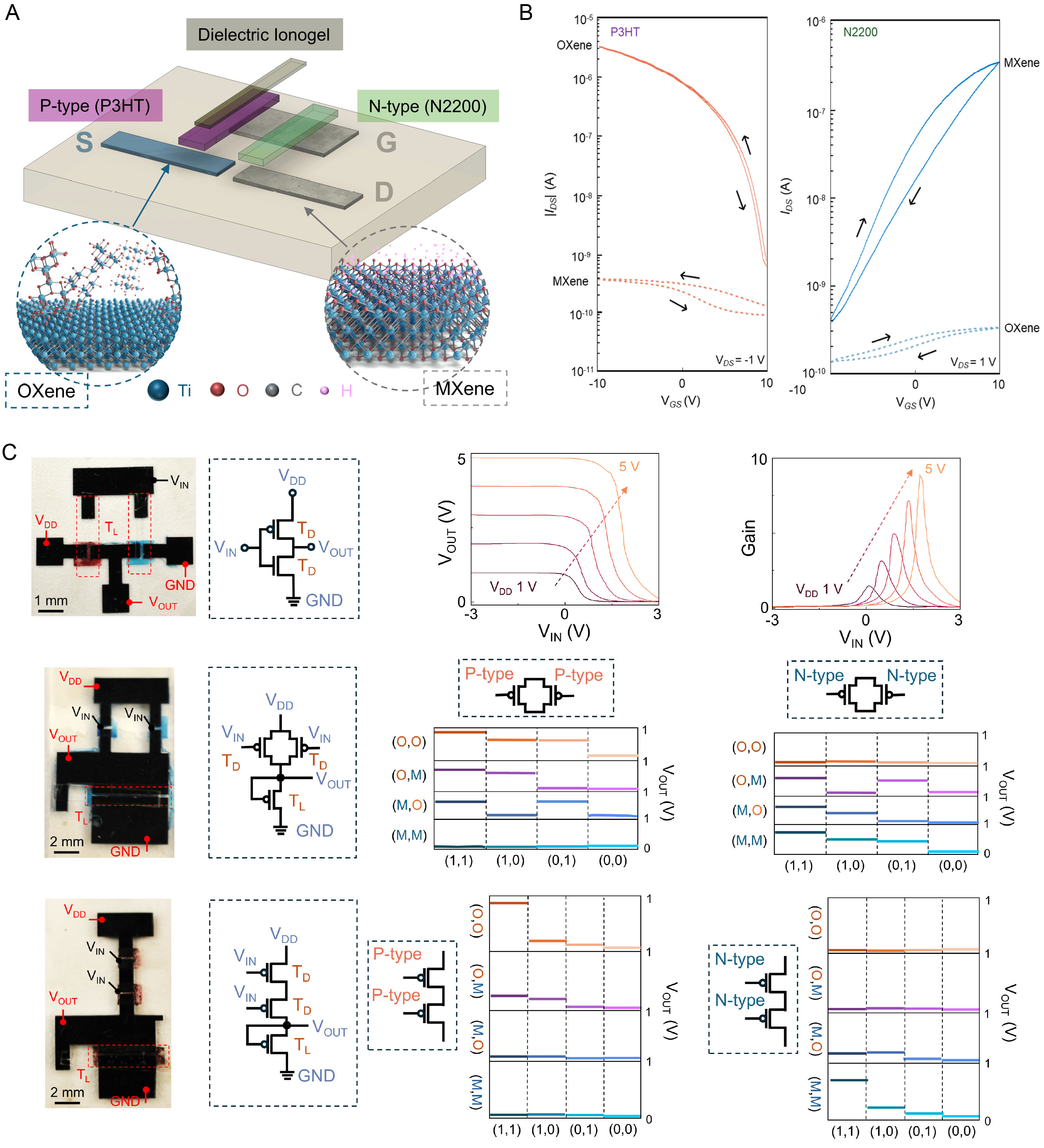
Figure 6. Dielectric ionogels for reconfigurable and contact-symmetry-engineered 2D nanoelectronics. (A) Schematic illustration of the reconfigurable field-effect transistors (FETs) gated by a high-capacitance dielectric ionogel layer, featuring complementary p-type (P3HT) and n-type (N2200) polymer semiconductor channels integrated onto symmetry-engineered asymmetric OXene contact electrodes; (B) Transfer characteristics (IDS-VGS) of transistors with a P3HT (P-type) and N2200 (N-type) semiconductor layer, respectively. The gate current around 10-12 A is omitted; (C) Reconfigurable P- and N-type logical circuits based on inverter, NAND gate, and NOR gate, including the input-output voltage and voltage gain characteristics. (A-C) Reproduced with permission from ref.[186], Copyright 2025, ACS. N2200: poly{[N,N′-bis(2-octyldodecyl)naphthalene-1,4,5,8-bis(dicarboximide)-2,6-diyl]-alt-5,5′-(2,2′-bithiophene)}; P3HT: poly(3-hexylthiophene).