

fig4
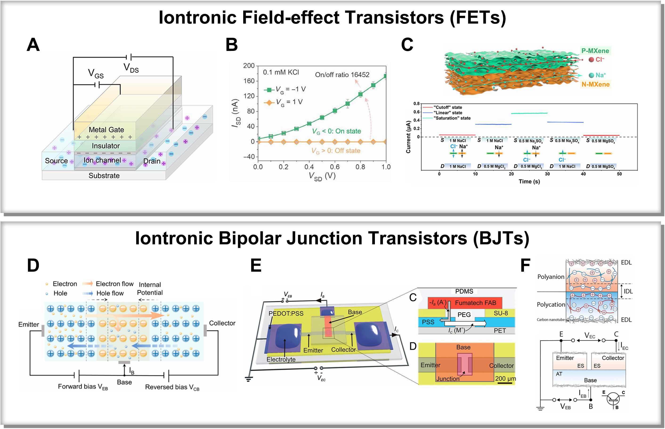
Figure 4. Iontronic transistors based on nanoconfined materials. (A) Concept schematic of iontronic field-effect transistors (iontronic FETs). This figure is quoted with permission from the American Chemical Society[25]; (B) The output curves of carbon-nanotube-based nanofluidic iontronic FET. This figure is quoted with permission from the American Association for the Advancement of Science[72]; (C) The output curves of NP-MXene-based iontronic FET. This figure is quoted with permission from the American Association for the Advancement of Science[70]; (D) Concept schematic of iontronic bipolar junction transistors (iontronic BJTs). This figure is quoted with permission from the American Chemical Society[25]; (E) Architecture of iontronic BJT based on ion-selective membranes. This figure is quoted with permission from the National Academy of Sciences[58]; (F) Schematic illustration of a polyanion/polycation junction architecture of an iontronic BJT based on ionoelastomers. This figure is quoted with permission from the American Association for the Advancement of Science[20]. EDL: Electrical double layer; IDL: ionic double layer; PEDOT:PSS: poly(3,4-ethylenedioxythiophene) :poly(styrenesulfonate); PET: polyethylene terephthalate; PEG: poly(ethylene glycol); ES: polyanionic ionoelastomer layer; AT: polycationic ionoelastomer layer; NP: negatively/positively; EB: emitter-base; CB: collector-base; PDMS: polydimethylsiloxane.