


fig3
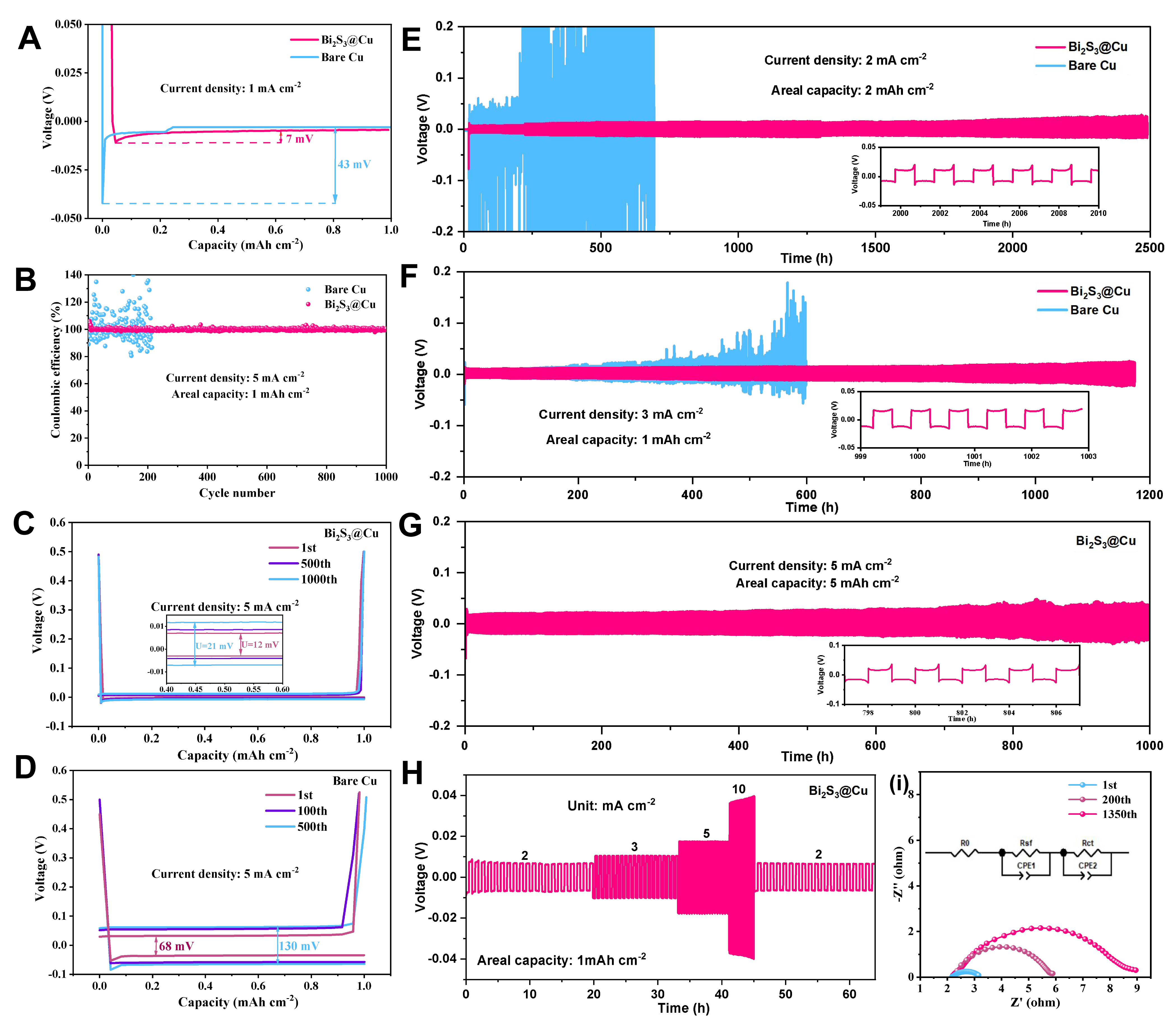
Figure 3. (A) Galvanostatic Na plating profiles on the bare Cu and Bi2S3@Cu substrates at 1 mA cm-2; (B) Comparison of CEs upon Na plating/stripping cycling on the Cu and Bi2S3@Cu substrates at 5 mA cm-2 and 1 mAh cm-2; (C and D) Voltage-capacity curves of sodium plating/stripping processes on Bi2S3@Cu substrate (C) and Cu substrate (D) at 5 mA cm-2; (E-G) Voltage-time profiles of symmetric cells of Na/Bi2S3@Cu and Na@Cu electrodes at (E) 2 mA cm-2 and 2 mAh cm-2, (F) 3 mA cm-2 and 1 mAh cm-2, and (G) 5 mA cm-2 and