


fig2
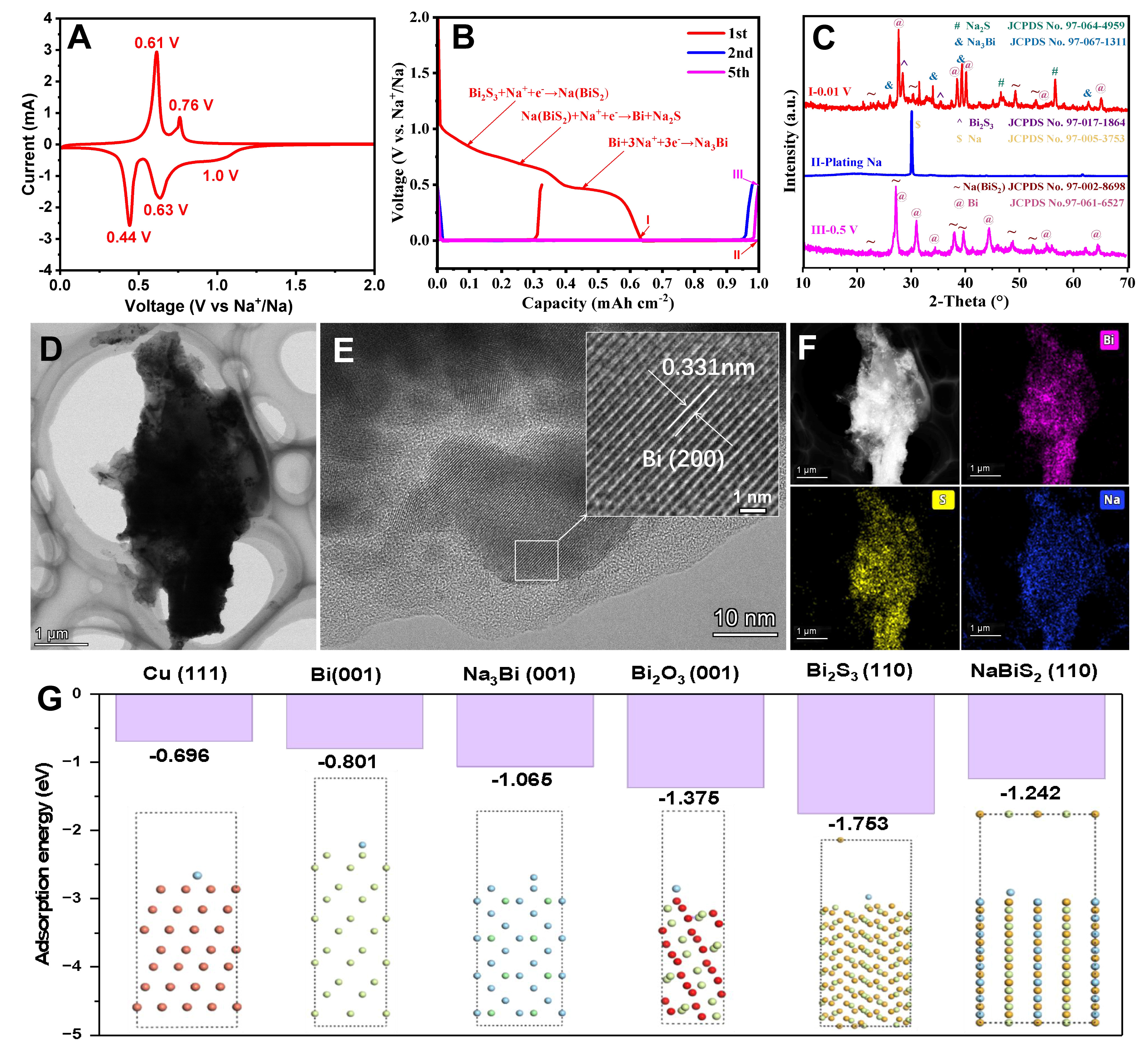
Figure 2. (A) Initial CV curve and (B) GCD curves of Bi2S3; (C) XRD patterns of the discharged Bi2S3 electrodes at different states; (D) TEM image and (E) HRTEM image of sodiated Bi2S3 at initially discharged to 0.5 V, and (F) HAADF-STEM image with corresponding EDS maps of Bi/S/Na elements; (G) Sodium adsorption energies on Cu (111), Bi (001), Na3Bi (001), Bi2O3 (001), Bi2S3 (110) and NaBiS2 (110) surfaces, where more negative values imply stronger adsorption. CV: Cyclic voltammetry; GCD: Galvanostatic discharge; XRD: X-ray diffraction; TEM: transmission electron microscope; HRTEM: high-resolution transmission electron microscopy; HAADF-STEM: high-resolution transmission electron microscopy; EDS: energy dispersive X-ray spectroscopy.