



fig2
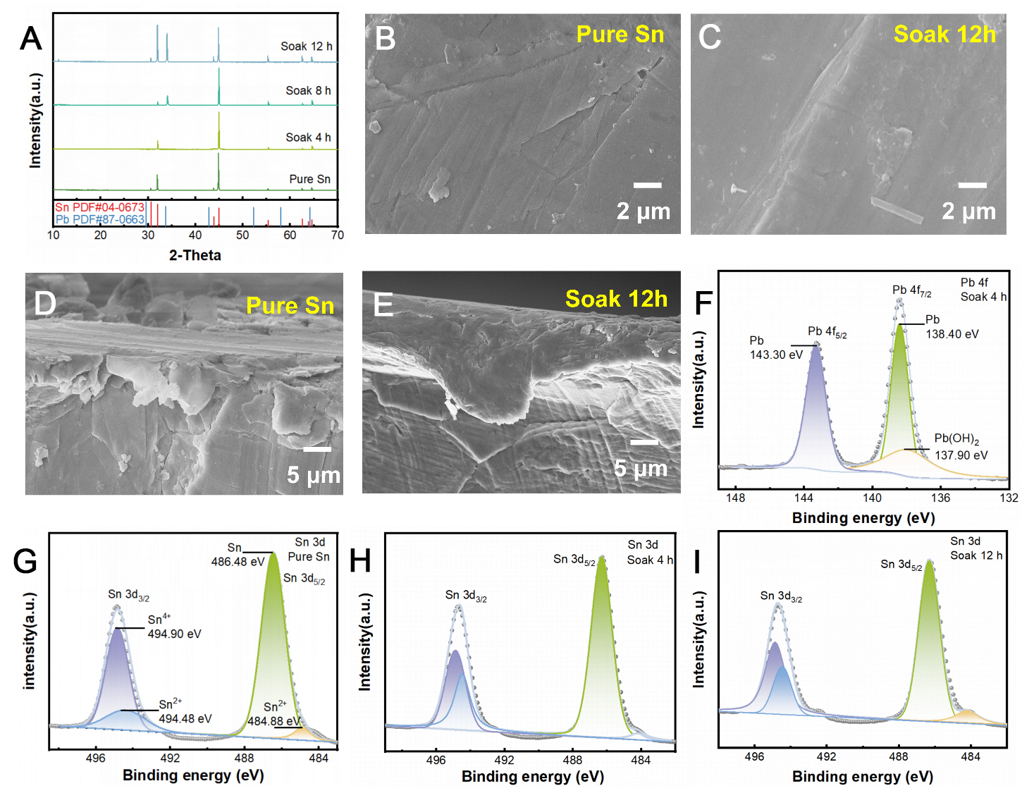
Figure 2. (A) XRD spectra of Pb@Sn negative electrode; SEM image of the surface of Pb@Sn anode: (B) Pure Sn and (C) Soak 12 h. Cross-sectional SEM images of tin sheets at different treatment times: (D) Pure Sn and (E) Soak 12 h. (F) XPS fitted curves of elemental Pb for Soak 4 h. XPS fitting curves for elemental Sn for (G) Pure Sn, (H) Soak 4 h, and (I) Soak 12 h samples. XRD: X-ray diffraction; SEM: scanning electron microscopy; XPS: X-ray photoelectron spectroscopy.